

Suprem III - Stanford Technology CAD Home Page
Suprem III - Stanford Technology CAD Home Page
Suprem III - Stanford Technology CAD Home Page

Create successful ePaper yourself
Turn your PDF publications into a flip-book with our unique Google optimized e-Paper software.
-179-<br />
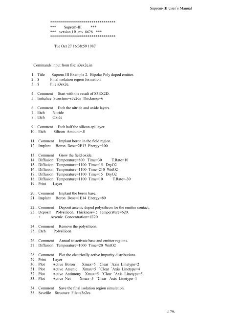
<strong>Suprem</strong>-<strong>III</strong> User´s Manual<br />
*********************************<br />
*** <strong>Suprem</strong>-<strong>III</strong> ***<br />
*** version 1B rev. 8628 ***<br />
*********************************<br />
Tue Oct 27 16:38:59 1987<br />
Commands input from file: s3ex2e.in<br />
1... Title <strong>Suprem</strong>-<strong>III</strong> Example 2. Bipolar Poly doped emitter.<br />
2... $ Final isolation region formation.<br />
3... $ File s3ex2e.<br />
4... Comment Start with the result of S3EX2D.<br />
5... Initialize Structure=s3e2ds Thickness=6<br />
6... Comment Etch the nitride and oxide layers.<br />
7... Etch Nitride<br />
8... Etch Oxide<br />
9... Comment Etch half the silicon epi layer.<br />
10... Etch Silicon Amount=.8<br />
11... Comment Implant boron in the field region.<br />
12... Implant Boron Dose=2E13 Energy=100<br />
13... Comment Grow the field oxide.<br />
14... Diffusion Temperature=800 Time=30 T.Rate=10<br />
15... Diffusion Temperature=1100 Time=15 DryO2<br />
16... Diffusion Temperature=1100 Time=210 WetO2<br />
17... Diffusion Temperature=1100 Time=15 DryO2<br />
18... Diffusion Temperature=1100 Time=10 T.Rate=-30<br />
19... Print Layer<br />
20... Comment Implant the boron base.<br />
21... Implant Boron Dose=1E14 Energy=80<br />
22... Comment Deposit arsenic doped polysilicon for the emitter contact.<br />
23... Deposit Polysilicon, Thickness=.5 Temperature=620.<br />
... + Arsenic Concentration=1E20<br />
24... Comment Remove the polysilicon.<br />
25... Etch Polysilicon<br />
26... Comment Anneal to activate base and emitter regions.<br />
27... Diffusion Temperature=1000 Time=20 WetO2<br />
28... Comment Plot the electrically active impurity distributions.<br />
29... Print Layer<br />
30... Plot Active Boron Xmax=5 Clear ˆAxis Linetype=2<br />
31... Plot Active Arsenic Xmax=5 ˆClear ˆAxis Linetype=4<br />
32... Plot Active Antimony Xmax=5 ˆClear ˆAxis Linetype=5<br />
33... Plot Active Net Xmax=5 ˆClear Axis Linetype=1<br />
34... Comment Save the final isolation region simulation.<br />
35... Savefile Structure File=s3e2es


