

Suprem III - Stanford Technology CAD Home Page
Suprem III - Stanford Technology CAD Home Page
Suprem III - Stanford Technology CAD Home Page

Create successful ePaper yourself
Turn your PDF publications into a flip-book with our unique Google optimized e-Paper software.
-152-<br />
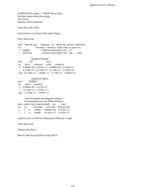
<strong>Suprem</strong>-<strong>III</strong> User´s Manual<br />
SUPREM-<strong>III</strong> Example 1. NMOS Silicon Gate<br />
Isolation region initial processing.<br />
File s3ex1e<br />
Initialize silicon substrate.<br />
Grow pad oxide, 400A.<br />
Implant boron to increase field region doping.<br />
Grow field oxide.<br />
layer material type thickness dx dxmin top bottom orientation<br />
no.<br />
(microns) (microns) node node or grain size<br />
2 OXIDE 0.7604 0.0100 0.0010 348 377<br />
1 SILICON 2.6654 0.0100 0.0010 378 500 <br />
Integrated Dopant<br />
layer Net Total<br />
no. active chemical active chemical<br />
2 0.0000e+00 -6.1674e+12 0.0000e+00 6.1674e+12<br />
1 -4.1330e+12 -4.1330e+12 4.1330e+12 4.1330e+12<br />
sum -4.1330e+12 -1.0300e+13 4.1330e+12 1.0300e+13<br />
Integrated Dopant<br />
layer BORON<br />
no. active chemical<br />
2 0.0000e+00 6.1674e+12<br />
1 4.1330e+12 4.1330e+12<br />
sum 4.1330e+12 1.0300e+13<br />
Junction Depths and Integrated Dopant<br />
Concentrations for Each Diffused Region<br />
layer region type junction depth net total<br />
no. no. (microns) active Qd chemical Qd<br />
2 1 p 0.0000 0.0000e+00 6.1674e+12<br />
1 1 p 0.0000 4.1330e+12 4.1330e+12<br />
Implant boron to shift the enhancement threshold voltage.<br />
Grow gate oxide<br />
Deposit polysilicon<br />
Heavily dope the polysilicon using POCl3


