

Suprem III - Stanford Technology CAD Home Page
Suprem III - Stanford Technology CAD Home Page
Suprem III - Stanford Technology CAD Home Page

You also want an ePaper? Increase the reach of your titles
YUMPU automatically turns print PDFs into web optimized ePapers that Google loves.
-175-<br />
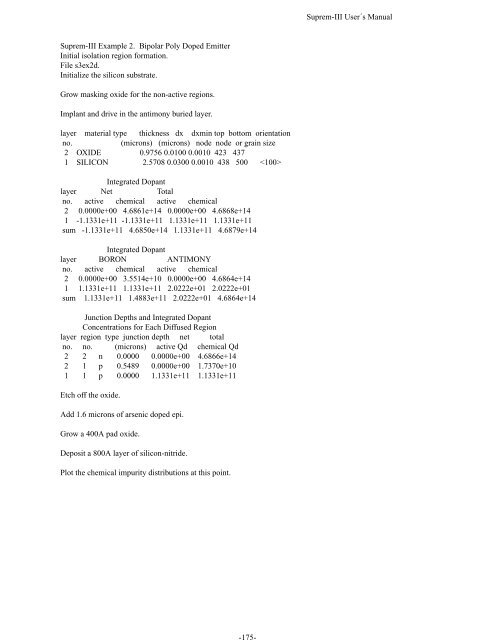
<strong>Suprem</strong>-<strong>III</strong> User´s Manual<br />
<strong>Suprem</strong>-<strong>III</strong> Example 2. Bipolar Poly Doped Emitter<br />
Initial isolation region formation.<br />
File s3ex2d.<br />
Initialize the silicon substrate.<br />
Grow masking oxide for the non-active regions.<br />
Implant and drive in the antimony buried layer.<br />
layer material type thickness dx dxmin top bottom orientation<br />
no.<br />
(microns) (microns) node node or grain size<br />
2 OXIDE 0.9756 0.0100 0.0010 423 437<br />
1 SILICON 2.5708 0.0300 0.0010 438 500 <br />
Integrated Dopant<br />
layer Net Total<br />
no. active chemical active chemical<br />
2 0.0000e+00 4.6861e+14 0.0000e+00 4.6868e+14<br />
1 -1.1331e+11 -1.1331e+11 1.1331e+11 1.1331e+11<br />
sum -1.1331e+11 4.6850e+14 1.1331e+11 4.6879e+14<br />
Integrated Dopant<br />
layer BORON ANTIMONY<br />
no. active chemical active chemical<br />
2 0.0000e+00 3.5514e+10 0.0000e+00 4.6864e+14<br />
1 1.1331e+11 1.1331e+11 2.0222e+01 2.0222e+01<br />
sum 1.1331e+11 1.4883e+11 2.0222e+01 4.6864e+14<br />
Junction Depths and Integrated Dopant<br />
Concentrations for Each Diffused Region<br />
layer region type junction depth net total<br />
no. no. (microns) active Qd chemical Qd<br />
2 2 n 0.0000 0.0000e+00 4.6866e+14<br />
2 1 p 0.5489 0.0000e+00 1.7370e+10<br />
1 1 p 0.0000 1.1331e+11 1.1331e+11<br />
Etch off the oxide.<br />
Add 1.6 microns of arsenic doped epi.<br />
Grow a 400A pad oxide.<br />
Deposit a 800A layer of silicon-nitride.<br />
Plot the chemical impurity distributions at this point.


