

Suprem III - Stanford Technology CAD Home Page
Suprem III - Stanford Technology CAD Home Page
Suprem III - Stanford Technology CAD Home Page

You also want an ePaper? Increase the reach of your titles
YUMPU automatically turns print PDFs into web optimized ePapers that Google loves.
-162-<br />
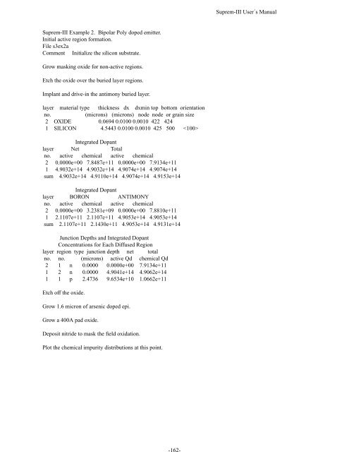
<strong>Suprem</strong>-<strong>III</strong> User´s Manual<br />
<strong>Suprem</strong>-<strong>III</strong> Example 2. Bipolar Poly doped emitter.<br />
Initial active region formation.<br />
File s3ex2a<br />
Comment Initialize the silicon substrate.<br />
Grow masking oxide for non-active regions.<br />
Etch the oxide over the buried layer regions.<br />
Implant and drive-in the antimony buried layer.<br />
layer material type thickness dx dxmin top bottom orientation<br />
no.<br />
(microns) (microns) node node or grain size<br />
2 OXIDE 0.0694 0.0100 0.0010 422 424<br />
1 SILICON 4.5443 0.0100 0.0010 425 500 <br />
Integrated Dopant<br />
layer Net Total<br />
no. active chemical active chemical<br />
2 0.0000e+00 7.8487e+11 0.0000e+00 7.9134e+11<br />
1 4.9032e+14 4.9032e+14 4.9074e+14 4.9074e+14<br />
sum 4.9032e+14 4.9110e+14 4.9074e+14 4.9153e+14<br />
Integrated Dopant<br />
layer BORON ANTIMONY<br />
no. active chemical active chemical<br />
2 0.0000e+00 3.2381e+09 0.0000e+00 7.8810e+11<br />
1 2.1107e+11 2.1107e+11 4.9053e+14 4.9053e+14<br />
sum 2.1107e+11 2.1430e+11 4.9053e+14 4.9131e+14<br />
Junction Depths and Integrated Dopant<br />
Concentrations for Each Diffused Region<br />
layer region type junction depth net total<br />
no. no. (microns) active Qd chemical Qd<br />
2 1 n 0.0000 0.0000e+00 7.9134e+11<br />
1 2 n 0.0000 4.9041e+14 4.9062e+14<br />
1 1 p 2.4736 9.6534e+10 1.0662e+11<br />
Etch off the oxide.<br />
Grow 1.6 micron of arsenic doped epi.<br />
Grow a 400A pad oxide.<br />
Deposit nitride to mask the field oxidation.<br />
Plot the chemical impurity distributions at this point.


