Suprem III - Stanford Technology CAD Home Page
Suprem III - Stanford Technology CAD Home Page
Suprem III - Stanford Technology CAD Home Page
Create successful ePaper yourself
Turn your PDF publications into a flip-book with our unique Google optimized e-Paper software.
-18-<br />
<strong>Suprem</strong>-<strong>III</strong> User´s Manual<br />
13. Bias Statement<br />
-----------------------<br />
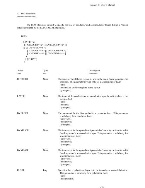
The BIAS statement is used to specify the bias of conductor and semiconductor layers during a Poisson<br />
solution initiated by the ELECTRICAL statement.<br />
BIAS<br />
LAYER=<br />
( [ V.ELECTR= ] [ DV.ELECTR= ] )<br />
| ( ( [ DIFFUSIO= ]<br />
[ V.MAJORI= ] [ DV.MAJOR= ]<br />
[ V.MINORI= ] [ DV.MINOR= ]<br />
)<br />
| [ FLOAT ]<br />
)<br />
Name Type Description<br />
---- ---- -----------<br />
DIFFUSIO Num The index of the diffused region for which the quasi-Fermi potentials are<br />
specified. The parameter is valid only for a semiconductor layer.<br />
(unit: )<br />
(default: All diffused regions in the layer.)<br />
(synonym: )<br />
LAYER Num The index of the conductor or semiconductor layer for which a bias is being<br />
specified.<br />
(unit: )<br />
(default: )<br />
(synonym: )<br />
DV.ELECT Num The increment for the bias applied to a conductor layer. This parameter<br />
is valid only for a conductor layer.<br />
(unit: volts.)<br />
(default: 0.0)<br />
(synonym: )<br />
DV.MAJOR Num The increment for the quasi-Fermi potential of majority carriers for a diffused<br />
region of a semiconductor layer. This parameter is valid only for<br />
a semiconductor layer.<br />
(unit: volts.)<br />
(default: 0.0)<br />
(synonym: )<br />
DV.MINOR Num The increment for the quasi-Fermi potential of minority carriers for a diffused<br />
region of a semiconductor layer. This parameter is valid only for<br />
a semiconductor layer.<br />
(unit: volts.)<br />
(default: 0.0)<br />
(synonym: )<br />
FLOAT Log Specifies that a polysilicon layer is to be treated as a neutral dielectric.<br />
This parameter is valid only for a polysilicon layer.<br />
(unit: )<br />
(default: false.)


