

Suprem III - Stanford Technology CAD Home Page
Suprem III - Stanford Technology CAD Home Page
Suprem III - Stanford Technology CAD Home Page

Create successful ePaper yourself
Turn your PDF publications into a flip-book with our unique Google optimized e-Paper software.
-181-<br />
<strong>Suprem</strong>-<strong>III</strong> User´s Manual<br />
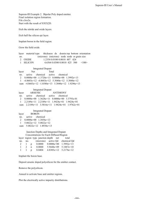
<strong>Suprem</strong>-<strong>III</strong> Example 2. Bipolar Poly doped emitter.<br />
Final isolation region formation.<br />
File s3ex2e.<br />
Start with the result of S3EX2D.<br />
Etch the nitride and oxide layers.<br />
Etch half the silicon epi layer.<br />
Implant boron in the field region.<br />
Grow the field oxide.<br />
layer material type thickness dx dxmin top bottom orientation<br />
no.<br />
(microns) (microns) node node or grain size<br />
2 OXIDE 1.2354 0.0100 0.0010 407 424<br />
1 SILICON 4.6564 0.0300 0.0010 425 500 <br />
Integrated Dopant<br />
layer Net Total<br />
no. active chemical active chemical<br />
2 0.0000e+00 -1.3720e+13 0.0000e+00 1.3992e+13<br />
1 -4.8603e+12 -4.8603e+12 5.3040e+12 5.3040e+12<br />
sum -4.8603e+12 -1.8580e+13 5.3040e+12 1.9296e+13<br />
Integrated Dopant<br />
layer ARSENIC ANTIMONY<br />
no. active chemical active chemical<br />
2 0.0000e+00 1.3628e+11 0.0000e+00 3.3793e-01<br />
1 2.2189e+11 2.2189e+11 1.9424e+01 1.9424e+01<br />
sum 2.2189e+11 3.5816e+11 1.9424e+01 1.9762e+01<br />
Integrated Dopant<br />
layer BORON<br />
no. active chemical<br />
2 0.0000e+00 1.3856e+13<br />
1 5.0822e+12 5.0822e+12<br />
sum 5.0822e+12 1.8938e+13<br />
Junction Depths and Integrated Dopant<br />
Concentrations for Each Diffused Region<br />
layer region type junction depth net total<br />
no. no. (microns) active Qd chemical Qd<br />
2 1 p 0.0000 0.0000e+00 1.3992e+13<br />
1 2 n 0.0000 5.9448e+09 5.1887e+10<br />
1 1 p 0.0404 4.8305e+12 5.2176e+12<br />
Implant the boron base.<br />
Deposit arsenic doped polysilicon for the emitter contact.<br />
Remove the polysilicon.<br />
Anneal to activate base and emitter regions.<br />
Plot the electrically active impurity distributions.


