

Suprem III - Stanford Technology CAD Home Page
Suprem III - Stanford Technology CAD Home Page
Suprem III - Stanford Technology CAD Home Page

You also want an ePaper? Increase the reach of your titles
YUMPU automatically turns print PDFs into web optimized ePapers that Google loves.
-167-<br />
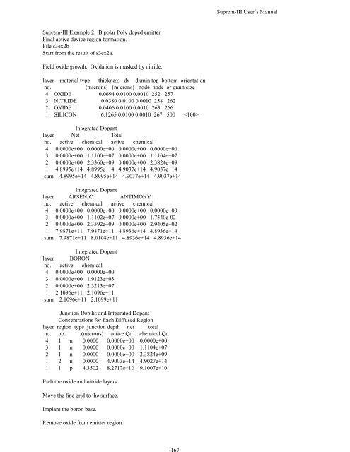
<strong>Suprem</strong>-<strong>III</strong> User´s Manual<br />
<strong>Suprem</strong>-<strong>III</strong> Example 2. Bipolar Poly doped emitter.<br />
Final active device region formation.<br />
File s3ex2b<br />
Start from the result of s3ex2a.<br />
Field oxide growth. Oxidation is masked by nitride.<br />
layer material type thickness dx dxmin top bottom orientation<br />
no.<br />
(microns) (microns) node node or grain size<br />
4 OXIDE 0.0694 0.0100 0.0010 252 257<br />
3 NITRIDE 0.0380 0.0100 0.0010 258 262<br />
2 OXIDE 0.0406 0.0100 0.0010 263 266<br />
1 SILICON 6.1265 0.0100 0.0010 267 500 <br />
Integrated Dopant<br />
layer Net Total<br />
no. active chemical active chemical<br />
4 0.0000e+00 0.0000e+00 0.0000e+00 0.0000e+00<br />
3 0.0000e+00 1.1100e+07 0.0000e+00 1.1104e+07<br />
2 0.0000e+00 2.3360e+09 0.0000e+00 2.3824e+09<br />
1 4.8995e+14 4.8995e+14 4.9037e+14 4.9037e+14<br />
sum 4.8995e+14 4.8995e+14 4.9037e+14 4.9037e+14<br />
Integrated Dopant<br />
layer ARSENIC ANTIMONY<br />
no. active chemical active chemical<br />
4 0.0000e+00 0.0000e+00 0.0000e+00 0.0000e+00<br />
3 0.0000e+00 1.1102e+07 0.0000e+00 1.7540e-02<br />
2 0.0000e+00 2.3592e+09 0.0000e+00 2.9405e+02<br />
1 7.9871e+11 7.9871e+11 4.8936e+14 4.8936e+14<br />
sum 7.9871e+11 8.0108e+11 4.8936e+14 4.8936e+14<br />
Integrated Dopant<br />
layer BORON<br />
no. active chemical<br />
4 0.0000e+00 0.0000e+00<br />
3 0.0000e+00 1.9123e+03<br />
2 0.0000e+00 2.3213e+07<br />
1 2.1096e+11 2.1096e+11<br />
sum 2.1096e+11 2.1099e+11<br />
Junction Depths and Integrated Dopant<br />
Concentrations for Each Diffused Region<br />
layer region type junction depth net total<br />
no. no. (microns) active Qd chemical Qd<br />
4 1 n 0.0000 0.0000e+00 0.0000e+00<br />
3 1 n 0.0000 0.0000e+00 1.1104e+07<br />
2 1 n 0.0000 0.0000e+00 2.3824e+09<br />
1 2 n 0.0000 4.9003e+14 4.9027e+14<br />
1 1 p 4.3502 8.2717e+10 9.1007e+10<br />
Etch the oxide and nitride layers.<br />
Move the fine grid to the surface.<br />
Implant the boron base.<br />
Remove oxide from emitter region.


