Chapter 10 Memory Subsystem.pdf
Chapter 10 Memory Subsystem.pdf
Chapter 10 Memory Subsystem.pdf
You also want an ePaper? Increase the reach of your titles
YUMPU automatically turns print PDFs into web optimized ePapers that Google loves.
Public Version<br />
General-Purpose <strong>Memory</strong> Controller www.ti.com<br />
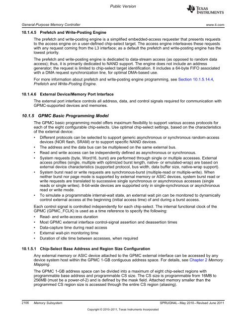
<strong>10</strong>.1.4.5 Prefetch and Write-Posting Engine<br />
The prefetch and write-posting engine is a simplified embedded-access requester that presents requests<br />
to the access engine on a user-defined chip-select target. The access engine interleaves these requests<br />
with any request coming from the L3 interface; as a default the prefetch and write-posting engine has the<br />
lowest priority.<br />
The prefetch and write-posting engine is dedicated to data-stream access (as opposed to random data<br />
access); thus, it is primarily dedicated to NAND support. The engine does not include an address<br />
generator; the request is limited to chip-select target identification. It includes a 64-byte FIFO associated<br />
with a DMA request synchronization line, for optimal DMA-based use.<br />
For more information about prefetch and write-posting engine programming, see Section <strong>10</strong>.1.5.14.4,<br />
Prefetch and Write-Posting Engine.<br />
<strong>10</strong>.1.4.6 External Device/<strong>Memory</strong> Port Interface<br />
The external port interface controls all address, data, and control signals required for communication with<br />
GPMC-supported devices and memories.<br />
<strong>10</strong>.1.5 GPMC Basic Programming Model<br />
The GPMC basic programming model offers maximum flexibility to support various access protocols for<br />
each of the eight configurable chip-selects. Use optimal chip-select settings, based on the characteristics<br />
of the external device:<br />
• Different protocols can be selected to support generic asynchronous or synchronous random-access<br />
devices (NOR flash, SRAM) or to support specific NAND devices.<br />
• The address and the data bus can be multiplexed on the same external bus.<br />
• Read and write access can be independently defined as asynchronous or synchronous.<br />
• System requests (byte, Word16, burst) are performed through single or multiple accesses. External<br />
access profiles (single, multiple with optimized burst length, native- or emulated-wrap) are based on<br />
external device characteristics (supported protocol, bus width, data buffer size, native-wrap support).<br />
• System burst read or write requests are synchronous-burst (multiple-read or multiple-write). When<br />
neither burst nor page mode is supported by external memory or ASIC devices, system burst read or<br />
write requests are translated to successive single synchronous or asynchronous accesses (single<br />
reads or single writes). 8-bit-wide devices are supported only in single-synchronous or asynchronous<br />
read or write mode.<br />
• To simulate a programmable internal-wait state, an external wait pin can be monitored to dynamically<br />
control external access at the beginning (initial access time) of and during a burst access.<br />
Each control signal is controlled independently for each chip-select. The internal functional clock of the<br />
GPMC (GPMC_FCLK) is used as a time reference to specify the following:<br />
• Read- and write-access duration<br />
• Most GPMC external interface control-signal assertion and deassertion times<br />
• Data-capture time during read access<br />
• External wait-pin monitoring time<br />
• Duration of idle time between accesses, when required<br />
<strong>10</strong>.1.5.1 Chip-Select Base Address and Region Size Configuration<br />
Any external memory or ASIC device attached to the GPMC external interface can be accessed by any<br />
device system host within the GPMC 1-GB contiguous address space. For details, see <strong>Chapter</strong> 2 <strong>Memory</strong><br />
Mapping.<br />
The GPMC 1-GB address space can be divided into a maximum of eight chip-select regions with<br />
programmable base address and programmable CS size. The CS size is programmable from 16MB to<br />
256MB (must be a power-of-2) and is defined by the mask field. Attached memory smaller than the<br />
programmed CS region size is accessed through the entire CS region (aliasing).<br />
2<strong>10</strong>6 <strong>Memory</strong> <strong>Subsystem</strong> SPRUGN4L–May 20<strong>10</strong>–Revised June 2011<br />
Copyright © 20<strong>10</strong>–2011, Texas Instruments Incorporated


