

Chapter 10 Memory Subsystem.pdf
Chapter 10 Memory Subsystem.pdf
Chapter 10 Memory Subsystem.pdf

You also want an ePaper? Increase the reach of your titles
YUMPU automatically turns print PDFs into web optimized ePapers that Google loves.
Public Version<br />
www.ti.com General-Purpose <strong>Memory</strong> Controller<br />
Bits Field Name Description Type Reset<br />
22:20 RESERVED Write 0s for future compatibility. Read returns 0s. RW 0x0<br />
19:16 WEONTIME nWE assertion time from start cycle time RW 0x3<br />
0x0: 0 GPMC_FCLK cycle<br />
0x1: 1 GPMC_FCLK cycle<br />
...<br />
0xF: 15 GPMC_FCLK cycles<br />
15:13 RESERVED Write 0s for future compatibility. Read returns 0s. RW 0x0<br />
12:8 OEOFFTIME nOE de-assertion time from start cycle time RW 0x<strong>10</strong><br />
0x00: 0 GPMC_FCLK cycle<br />
0x01: 1 GPMC_FCLK cycle<br />
...<br />
0x1F: 31 GPMC_FCLK cycles<br />
7 OEEXTRADELAY nOE Add Extra Half GPMC_FCLK cycle RW 0x0<br />
0x0: nOE Timing control signal is not delayed<br />
0x1: nOE Timing control signal is delayed of half GPMC_FCLK<br />
clock cycle<br />
6:4 RESERVED Write 0s for future compatibility. Read returns 0s. RW 0x0<br />
3:0 OEONTIME nOE assertion time from start cycle time RW 0x3<br />
0x0: 0 GPMC_FCLK cycle<br />
0x1: 1 GPMC_FCLK cycle<br />
...<br />
0xF: 15 GPMC_FCLK cycles<br />
Table <strong>10</strong>-56. Register Call Summary for Register GPMC_CONFIG4_i<br />
General-Purpose <strong>Memory</strong> Controller<br />
• Timing Setting: [0] [1] [2] [3] [4] [5]<br />
• Asynchronous Access Description: [6] [7] [8] [9] [<strong>10</strong>] [11]<br />
• Synchronous Access: [12] [13] [14] [15] [16] [17]<br />
• NAND Device Basic Programming Model: [18]<br />
• GPMC Register Summary: [19]<br />
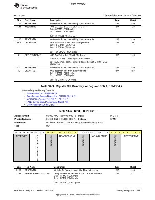
Table <strong>10</strong>-57. GPMC_CONFIG5_i<br />
Address Offset 0x0000 0070 + (0x0000 0030 * i) Index i = 0 to 7<br />
Physical Address 0x6E00 0070 + (0x0000 0030 * i) Instance GPMC<br />
Description RdAccessTime and CycleTime timing parameters configuration<br />
Type RW<br />
31 30 29 28 27 26 25 24 23 22 21 20 19 18 17 16 15 14 13 12 11 <strong>10</strong> 9 8 7 6 5 4 3 2 1 0<br />
RESERVED RDACCESSTIME WRCYCLETIME RDCYCLETIME<br />
PAGEBURSTACCESSTIME<br />
RESERVED<br />
Bits Field Name Description Type Reset<br />
31:28 RESERVED Write 0s for future compatibility. Read returns 0s. RW 0x0<br />
27:24 PAGEBURSTACCESSTIME Delay between successive words in a multiple access RW 0x1<br />
0x0: 0 GPMC_FCLK cycle<br />
0x1: 1 GPMC_FCLK cycle<br />
...<br />
0xF: 15 GPMC_FCLK cycles<br />
SPRUGN4L–May 20<strong>10</strong>–Revised June 2011 <strong>Memory</strong> <strong>Subsystem</strong><br />
RESERVED<br />
Copyright © 20<strong>10</strong>–2011, Texas Instruments Incorporated<br />
RESERVED<br />
2191


