

Chapter 10 Memory Subsystem.pdf
Chapter 10 Memory Subsystem.pdf
Chapter 10 Memory Subsystem.pdf

Create successful ePaper yourself
Turn your PDF publications into a flip-book with our unique Google optimized e-Paper software.
GPMC_FCLK<br />
GPMC_CLK<br />
gpmc_a[11:1]<br />
(connected to A [26:17] on memory side)<br />
gpmc_d[15:0]<br />
(connected to A [16:1] / D [15:0] on<br />
memory side)<br />
nBE1/nBE0<br />
nCS<br />
nADV<br />
nWE<br />
DIR<br />
WAIT<br />
CSONTIME<br />
Valid Address<br />
WRDATAONADMUXBUS<br />
Valid Address Data<br />
CSWROFFTIME<br />
ADVWROFFTIME<br />
ADVONTIME<br />
WEOFFTIME<br />
WEONTIME<br />
Public Version<br />
General-Purpose <strong>Memory</strong> Controller www.ti.com<br />
• Total access time (GPMC.GPMC_CONFIG5_i[4:0] RDCYCLETIME) corresponds to RDACCESSTIME<br />
plus the address hold time from nCS deassertion, plus time from RDACCESSTIME to<br />
CSWROFFTIME.<br />
• Direction signal DIR:<br />
DIR goes from OUT to IN at the same time as nOE assertion.<br />
After a read operation, if no other access (read or write) is pending, the data bus is driven with the<br />
previous read value. See Section <strong>10</strong>.1.5.3.<strong>10</strong>, Bus Keeping Support.<br />
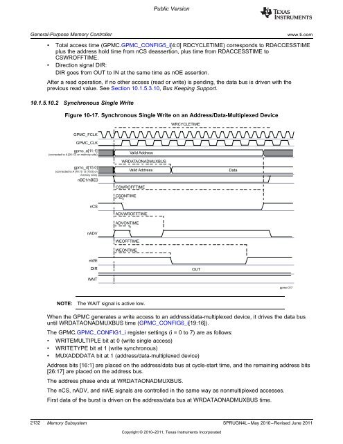
<strong>10</strong>.1.5.<strong>10</strong>.2 Synchronous Single Write<br />
Figure <strong>10</strong>-17. Synchronous Single Write on an Address/Data-Multiplexed Device<br />
NOTE: The WAIT signal is active low.<br />
WRCYCLETIME<br />
When the GPMC generates a write access to an address/data-multiplexed device, it drives the data bus<br />
until WRDATAONADMUXBUS time (GPMC_CONFIG6_i[19:16]).<br />
The GPMC.GPMC_CONFIG1_i register settings (i = 0 to 7) are as follows:<br />
OUT<br />
• WRITEMULTIPLE bit at 0 (write single access)<br />
• WRITETYPE bit at 1 (write synchronous)<br />
• MUXADDDATA bit at 1 (address/data-multiplexed device)<br />
Address bits [16:1] are placed on the address/data bus at cycle-start time, and the remaining address bits<br />
[26:17] are placed on the address bus.<br />
The address phase ends at WRDATAONADMUXBUS.<br />
The nCS, nADV, and nWE signals are controlled in the same way as nonmultiplexed accesses.<br />
First data of the burst is driven on the address/data bus at WRDATAONADMUXBUS time.<br />
2132 <strong>Memory</strong> <strong>Subsystem</strong> SPRUGN4L–May 20<strong>10</strong>–Revised June 2011<br />
Copyright © 20<strong>10</strong>–2011, Texas Instruments Incorporated<br />
gpmc-017


