

Chapter 10 Memory Subsystem.pdf
Chapter 10 Memory Subsystem.pdf
Chapter 10 Memory Subsystem.pdf

You also want an ePaper? Increase the reach of your titles
YUMPU automatically turns print PDFs into web optimized ePapers that Google loves.
FCLK<br />
nCS<br />
nADV<br />
nOE<br />
A/D bus<br />
AdvRdOffTime = 1<br />
OeOnTime = 3<br />
Valid Address<br />
Data capture on GPMC side: AccessTime = 9<br />
CsReadOffTime = <strong>10</strong><br />
OeOffTime = <strong>10</strong><br />
<strong>Memory</strong>-side access time<br />
Public Version<br />
General-Purpose <strong>Memory</strong> Controller www.ti.com<br />
In the following section i stands for the chip-select number, i = 0 to 7.<br />
• GPMC.GPMC_CONFIG[1] LIMITEDADDRESS set to 1 (A26-A11 are not modified during an external<br />
memory access)<br />
• GPMC.GPMC_CONFIG1_i register settings:<br />
– GPMC_CONFIG1_i[30] READMULTIPLE bit at 0 (read single access)<br />
– GPMC_CONFIG1_i[29] READTYPE bit at 0 (asynchronous read)<br />
– GPMC_CONFIG1_i[9] MUXADDDATA bit at 0 (non multiplexed device)<br />
• Chip-select signal nCS:<br />
– nCS assertion time is controlled by the GPMC_CONFIG2_i[3:0] CSONTIME field. It controls the<br />
address setup time to nCS assertion.<br />
– nCS deassertion time is controlled by the GPMC_CONFIG2_i[12:8] CSRDOFFTIME field. It<br />
controls the address hold time from nCS deassertion.<br />
• Address valid signal nADV:<br />
– nADV assertion time is controlled by the GPMC_CONFIG3_i[3:0] ADVONTIME field.<br />
– nADV deassertion time is controlled by the GPMC_CONFIG3_i[12:8] ADVRDOFFTIME field.<br />
• Output enable signal nOE:<br />
– nOE assertion indicates a read cycle.<br />
– nOE assertion time is controlled by the GPMC_CONFIG4_i[3:0] OEONTIME field.<br />
– nOE deassertion time is controlled by the GPMC_CONFIG4_i[12:8] OEOFFTIME field.<br />
• Read data is latched when RDACCESSTIME completes. Access time is defined in the<br />
GPMC.GPMC_CONFIG5_i[20:16] RDACCESSTIME field.<br />
• The end of the access is defined by the RDCYCLETIME parameter. The read cycle time is defined in<br />
the GPMC.GPMC_CONFIG5_i[4:0] RDCYCLETIME field.<br />
• Direction signal DIR: DIR goes from OUT to IN at the same time that nOE is asserted.<br />
After a read operation, if no other access (read or write) is pending, the data bus is driven with the<br />
previous read value. See Section <strong>10</strong>.1.5.3.<strong>10</strong>, Bus Keeping Support for more details.<br />
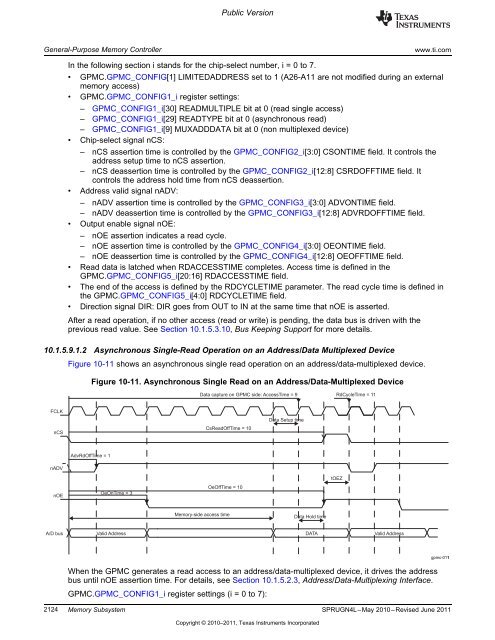
<strong>10</strong>.1.5.9.1.2 Asynchronous Single-Read Operation on an Address/Data Multiplexed Device<br />
Figure <strong>10</strong>-11 shows an asynchronous single read operation on an address/data-multiplexed device.<br />
Figure <strong>10</strong>-11. Asynchronous Single Read on an Address/Data-Multiplexed Device<br />
Data Setup time<br />
Data Hold time<br />
DATA<br />
RdCycleTime = 11<br />
tOEZ<br />
Valid Address<br />
When the GPMC generates a read access to an address/data-multiplexed device, it drives the address<br />
bus until nOE assertion time. For details, see Section <strong>10</strong>.1.5.2.3, Address/Data-Multiplexing Interface.<br />
GPMC.GPMC_CONFIG1_i register settings (i = 0 to 7):<br />
2124 <strong>Memory</strong> <strong>Subsystem</strong> SPRUGN4L–May 20<strong>10</strong>–Revised June 2011<br />
Copyright © 20<strong>10</strong>–2011, Texas Instruments Incorporated<br />
gpmc-011


