Chapter 10 Memory Subsystem.pdf
Chapter 10 Memory Subsystem.pdf
Chapter 10 Memory Subsystem.pdf
You also want an ePaper? Increase the reach of your titles
YUMPU automatically turns print PDFs into web optimized ePapers that Google loves.
Public Version<br />
General-Purpose <strong>Memory</strong> Controller www.ti.com<br />
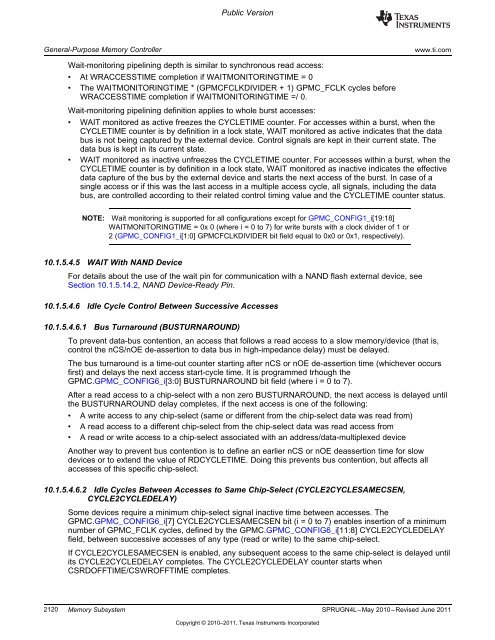
Wait-monitoring pipelining depth is similar to synchronous read access:<br />
• At WRACCESSTIME completion if WAITMONITORINGTIME = 0<br />
• The WAITMONITORINGTIME * (GPMCFCLKDIVIDER + 1) GPMC_FCLK cycles before<br />
WRACCESSTIME completion if WAITMONITORINGTIME =/ 0.<br />
Wait-monitoring pipelining definition applies to whole burst accesses:<br />
• WAIT monitored as active freezes the CYCLETIME counter. For accesses within a burst, when the<br />
CYCLETIME counter is by definition in a lock state, WAIT monitored as active indicates that the data<br />
bus is not being captured by the external device. Control signals are kept in their current state. The<br />
data bus is kept in its current state.<br />
• WAIT monitored as inactive unfreezes the CYCLETIME counter. For accesses within a burst, when the<br />
CYCLETIME counter is by definition in a lock state, WAIT monitored as inactive indicates the effective<br />
data capture of the bus by the external device and starts the next access of the burst. In case of a<br />
single access or if this was the last access in a multiple access cycle, all signals, including the data<br />
bus, are controlled according to their related control timing value and the CYCLETIME counter status.<br />
NOTE: Wait monitoring is supported for all configurations except for GPMC_CONFIG1_i[19:18]<br />
WAITMONITORINGTIME = 0x 0 (where i = 0 to 7) for write bursts with a clock divider of 1 or<br />
2 (GPMC_CONFIG1_i[1:0] GPMCFCLKDIVIDER bit field equal to 0x0 or 0x1, respectively).<br />
<strong>10</strong>.1.5.4.5 WAIT With NAND Device<br />
For details about the use of the wait pin for communication with a NAND flash external device, see<br />
Section <strong>10</strong>.1.5.14.2, NAND Device-Ready Pin.<br />
<strong>10</strong>.1.5.4.6 Idle Cycle Control Between Successive Accesses<br />
<strong>10</strong>.1.5.4.6.1 Bus Turnaround (BUSTURNAROUND)<br />
To prevent data-bus contention, an access that follows a read access to a slow memory/device (that is,<br />
control the nCS/nOE de-assertion to data bus in high-impedance delay) must be delayed.<br />
The bus turnaround is a time-out counter starting after nCS or nOE de-assertion time (whichever occurs<br />
first) and delays the next access start-cycle time. It is programmed trhough the<br />
GPMC.GPMC_CONFIG6_i[3:0] BUSTURNAROUND bit field (where i = 0 to 7).<br />
After a read access to a chip-select with a non zero BUSTURNAROUND, the next access is delayed until<br />
the BUSTURNAROUND delay completes, if the next access is one of the following:<br />
• A write access to any chip-select (same or different from the chip-select data was read from)<br />
• A read access to a different chip-select from the chip-select data was read access from<br />
• A read or write access to a chip-select associated with an address/data-multiplexed device<br />
Another way to prevent bus contention is to define an earlier nCS or nOE deassertion time for slow<br />
devices or to extend the value of RDCYCLETIME. Doing this prevents bus contention, but affects all<br />
accesses of this specific chip-select.<br />
<strong>10</strong>.1.5.4.6.2 Idle Cycles Between Accesses to Same Chip-Select (CYCLE2CYCLESAMECSEN,<br />
CYCLE2CYCLEDELAY)<br />
Some devices require a minimum chip-select signal inactive time between accesses. The<br />
GPMC.GPMC_CONFIG6_i[7] CYCLE2CYCLESAMECSEN bit (i = 0 to 7) enables insertion of a minimum<br />
number of GPMC_FCLK cycles, defined by the GPMC.GPMC_CONFIG6_i[11:8] CYCLE2CYCLEDELAY<br />
field, between successive accesses of any type (read or write) to the same chip-select.<br />
If CYCLE2CYCLESAMECSEN is enabled, any subsequent access to the same chip-select is delayed until<br />
its CYCLE2CYCLEDELAY completes. The CYCLE2CYCLEDELAY counter starts when<br />
CSRDOFFTIME/CSWROFFTIME completes.<br />
2120 <strong>Memory</strong> <strong>Subsystem</strong> SPRUGN4L–May 20<strong>10</strong>–Revised June 2011<br />
Copyright © 20<strong>10</strong>–2011, Texas Instruments Incorporated


