

Chapter 10 Memory Subsystem.pdf
Chapter 10 Memory Subsystem.pdf
Chapter 10 Memory Subsystem.pdf

You also want an ePaper? Increase the reach of your titles
YUMPU automatically turns print PDFs into web optimized ePapers that Google loves.
GPMC_FCLK<br />
GPMC_CLK<br />
gpmc_a[11:1]<br />
(connected to A [9:0] on memory side)<br />
gpmc_d[15:0]<br />
(connected to D [15:0] on memory side)<br />
nBE1/nBE0<br />
nCS<br />
nADV<br />
nOE<br />
DIR<br />
WAIT<br />
CLKACTIVATIONTIME<br />
CSONTIME<br />
ADVONTIME<br />
Valid Address<br />
ADVRDOFFTIME<br />
OEONTIME<br />
Valid Address<br />
Public Version<br />
General-Purpose <strong>Memory</strong> Controller www.ti.com<br />
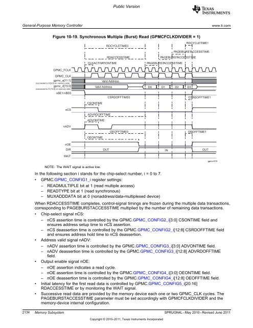
Figure <strong>10</strong>-19. Synchronous Multiple (Burst) Read (GPMCFCLKDIVIDER = 1)<br />
NOTE: The WAIT signal is active low.<br />
RDCYCLETIME0<br />
RDACCESSTIME<br />
CSRDOFFTIME0<br />
OEOFFTIME0<br />
PAGEBURSTACCESSTIME<br />
PAGEBURSTACCESSTIME<br />
D0 D1 D2 D3<br />
RDCYCLETIME1<br />
PAGEBURSTACCESSTIME<br />
CSRDOFFTIME1<br />
OEOFFTIME1<br />
OUT IN OUT<br />
In the following section i stands for the chip-select number, i = 0 to 7.<br />
• GPMC.GPMC_CONFIG1_i register settings:<br />
– READMULTIPLE bit at 1 (read multiple access)<br />
– READTYPE bit at 1 (read synchronous)<br />
– MUXADDDATA bit at 0 (nonaddress/data-multiplexed device)<br />
When RDACCESSTIME completes, control-signal timings are frozen during the multiple data transactions,<br />
corresponding to PAGEBURSTACCESSTIME multiplied by the number of remaining data transactions.<br />
• Chip-select signal nCS:<br />
– nCS assertion time is controlled by the GPMC.GPMC_CONFIG2_i[3:0] CSONTIME field and<br />
ensures address setup time to nCS assertion.<br />
– nCS deassertion time is controlled by the GPMC.GPMC_CONFIG2_i[12:8] CSRDOFFTIME field<br />
and ensures address hold time to nCS deassertion.<br />
• Address valid signal nADV:<br />
– nADV assertion time is controlled by the GPMC.GPMC_CONFIG3_i[3:0] ADVONTIME field.<br />
– nADV deassertion time is controlled by the GPMC.GPMC_CONFIG3_i[12:8] ADVRDOFFTIME<br />
field.<br />
• Output enable signal nOE:<br />
– nOE assertion indicates a read cycle.<br />
– nOE assertion time is controlled by the GPMC.GPMC_CONFIG4_i[3:0] OEONTIME field.<br />
– nOE deassertion time is controlled by the GPMC.GPMC_CONFIG4_i[12:8] OEOFFTIME field.<br />
• Initial latency for the first read data is controlled by GPMC.GPMC_CONFIG5_i[20:16]<br />
RDACCESSTIME or by monitoring the WAIT signal.<br />
• Successive read data are provided by the memory device each one or two GPMC_CLK cycles. The<br />
PAGEBURSTACCESSTIME parameter must be set accordingly with GPMCFCLKDIVIDER and the<br />
memory-device internal configuration.<br />
2134 <strong>Memory</strong> <strong>Subsystem</strong> SPRUGN4L–May 20<strong>10</strong>–Revised June 2011<br />
Copyright © 20<strong>10</strong>–2011, Texas Instruments Incorporated<br />
gpmc-019


