

Chapter 10 Memory Subsystem.pdf
Chapter 10 Memory Subsystem.pdf
Chapter 10 Memory Subsystem.pdf

Create successful ePaper yourself
Turn your PDF publications into a flip-book with our unique Google optimized e-Paper software.
GPMC_FCLK<br />
GPMC_CLK<br />
gpmc_a[11:1]<br />
(connected to A[<strong>10</strong>:1]] on<br />
memory side)<br />
gpmc_d[15:0]<br />
(connected to D[15:0] on<br />
memory side)<br />
nBE1/nBE0<br />
nCS<br />
nADV<br />
nWE<br />
WAIT<br />
CSWROFFTIME<br />
CSONTIME<br />
ADVWROFFTIME<br />
ADVONTIME<br />
WEOFFTIME<br />
WEONTIME<br />
Public Version<br />
General-Purpose <strong>Memory</strong> Controller www.ti.com<br />
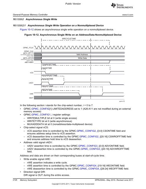
<strong>10</strong>.1.5.9.2 Asynchronous Single Write<br />
<strong>10</strong>.1.5.9.2.1 Asynchronous Single Write Operation on a Nonmultiplexed Device<br />
Figure <strong>10</strong>-12 shows an asynchronous single write operation on a nonmultiplexed device.<br />
Figure <strong>10</strong>-12. Asynchronous Single Write on an Address/Data-Nonmultiplexed Device<br />
WRCYCLETIME<br />
Valid Address<br />
Write Data<br />
In the following section i stands for the chip-select number, i = 0 to 7.<br />
• GPMC.GPMC_CONFIG[1] LIMITEDADDRESS set to 1 (A26-A11 are not modified during an external<br />
memory access)<br />
• GPMC.GPMC_CONFIG1_i register settings:<br />
– WRITEMULTIPLE bit at 0 (write single access)<br />
– WRITETYPE bit at 0 (write asynchronous)<br />
– MUXADDDATA bit at 0 (nonaddress/data-multiplexed device)<br />
• Chip-select signal nCS:<br />
– nCS assertion time is controlled by the GPMC.GPMC_CONFIG2_i[3:0] CSONTIME field and<br />
ensures address setup time to nCS assertion.<br />
– nCS deassertion time is controlled by the GPMC.GPMC_CONFIG2_i[20:16] CSWROFFTIME field<br />
and ensures address hold time to nCS deassertion.<br />
• Address valid signal nADV:<br />
gpmc-012<br />
– nADV assertion time is controlled by the GPMC.GPMC_CONFIG3_i[3:0] ADVONTIME field.<br />
– nADV deassertion time is controlled by the GPMC.GPMC_CONFIG3_i[20:16] ADVWROFFTIME<br />
field.<br />
Address and data are driven on their corresponding buses at start-of-cycle time.<br />
• Write enable signal nWE:<br />
– nWE assertion indicates a write cycle.<br />
– nWE assertion time is controlled by the GPMC.GPMC_CONFIG4_i[19:16] WEONTIME field.<br />
– nWE deassertion time is controlled by the GPMC.GPMC_CONFIG4_i[28:24] WEOFFTIME field.<br />
• Direction signal DIR:<br />
DIR signal is OUT during the entire access.<br />
2126 <strong>Memory</strong> <strong>Subsystem</strong> SPRUGN4L–May 20<strong>10</strong>–Revised June 2011<br />
Copyright © 20<strong>10</strong>–2011, Texas Instruments Incorporated


