

Geode GXLV Processor Series Low Power Integrated x86 Solutions
Geode GXLV Processor Series Low Power Integrated x86 Solutions
Geode GXLV Processor Series Low Power Integrated x86 Solutions

You also want an ePaper? Increase the reach of your titles
YUMPU automatically turns print PDFs into web optimized ePapers that Google loves.
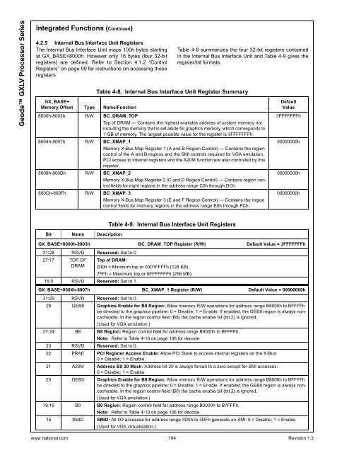
<strong>Geode</strong> <strong>GXLV</strong> <strong>Processor</strong> <strong>Series</strong><strong>Integrated</strong> Functions (Continued)4.2.5 Internal Bus Interface Unit RegistersThe Internal Bus Interface Unit maps 100h bytes startingat GX_BASE+8000h. However only 16 bytes (four 32-bitregisters) are defined. Refer to Section 4.1.2 “ControlRegisters” on page 99 for instructions on accessing theseregisters.Table 4-8 summarizes the four 32-bit registers containedin the Internal Bus Interface Unit and Table 4-9 gives theregister/bit formats.Table 4-8. Internal Bus Interface Unit Register SummaryGX_BASE+Memory Offset Type Name/Function8000h-8003h R/W BC_DRAM_TOPTop of DRAM — Contains the highest available address of system memory notincluding the memory that is set aside for graphics memory, which corresponds to1 GB of memory. The largest possible value for the register is 3FFFFFFFh.8004h-8007h R/W BC_XMAP_1Memory X-Bus Map Register 1 (A and B Region Control) — Contains the regioncontrol of the A and B regions and the SMI controls required for VGA emulation.PCI access to internal registers and the A20M function are also controlled by thisregister.8008h-800Bh R/W BC_XMAP_2Memory X-Bus Map Register 2 (C and D Region Control) — Contains region controlfields for eight regions in the address range C0h through DCh.800Ch-800Fh R/W BC_XMAP_3Memory X-Bus Map Register 3 (E and F Region Control) — Contains the regioncontrol fields for memory regions in the address range E0h through FCh.DefaultValue3FFFFFFFh00000000h00000000h00000000hBit Name DescriptionTable 4-9. Internal Bus Interface Unit RegistersGX_BASE+8000h-8003h BC_DRAM_TOP Register (R/W) Default Value = 3FFFFFFFh31:28 RSVD Reserved: Set to 0.27:17 TOP OFDRAMTop of DRAM:000h = Minimum top or 0001FFFFh (128 KB).7FFh = Maximum top or 0FFFFFFFh (256 MB).16:0 RSVD Reserved: Set to 1.GX_BASE+8004h-8007h BC_XMAP_1 Register (R/W) Default Value = 00000000h31:29 RSVD Reserved: Set to 0.28 GEB8 Graphics Enable for B8 Region: Allow memory R/W operations for address range B8000h to BFFFFhbe directed to the graphics pipeline: 0 = Disable; 1 = Enable. If enabled, the GEB8 region is always noncacheable.In the region control field (B8) the cache enable bit (bit 2) is ignored.(Used for VGA emulation.)27:24 B8 B8 Region: Region control field for address range B8000h to BFFFFh.Note: Refer to Table 4-10 on page 106 for decode.23 RSVD Reserved: Set to 0.22 PRAE PCI Register Access Enable: Allow PCI Slave to access internal registers on the X-Bus:0 = Disable; 1 = Enable.21 A20M Address Bit 20 Mask: Address bit 20 is always forced to a zero except for SMI accesses:0 = Disable; 1 = Enable.20 GEB0 Graphics Enable for B0 Region: Allow memory R/W operations for address range B8000h to BFFFFhbe directed to the graphics pipeline: 0 = Disable; 1 = Enable. If enabled, the GEB0 region is always noncacheable.In the region control field (B0) the cache enable bit (bit 2) is ignored.(Used for VGA emulation.)19:16 B0 B0 Region: Region control field for address range B0000h to B7FFFh.Note: Refer to Table 4-10 on page 106 for decode.15 SMID SMID: All I/O accesses for address range 3D0h to 3DFh generate an SMI: 0 = Disable; 1 = Enable.(Used for VGA virtualization.)www.national.com 104 Revision 1.3


