

Geode GXLV Processor Series Low Power Integrated x86 Solutions
Geode GXLV Processor Series Low Power Integrated x86 Solutions
Geode GXLV Processor Series Low Power Integrated x86 Solutions

Create successful ePaper yourself
Turn your PDF publications into a flip-book with our unique Google optimized e-Paper software.
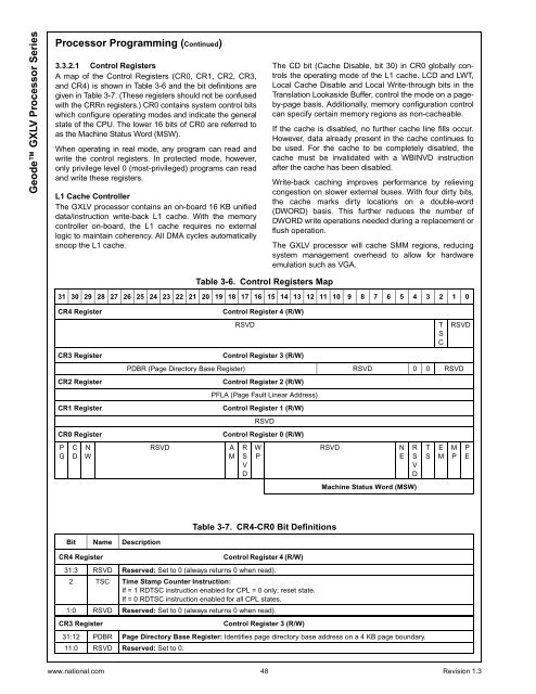
<strong>Geode</strong> <strong>GXLV</strong> <strong>Processor</strong> <strong>Series</strong><strong>Processor</strong> Programming (Continued)3.3.2.1 Control RegistersA map of the Control Registers (CR0, CR1, CR2, CR3,and CR4) is shown in Table 3-6 and the bit definitions aregiven in Table 3-7. (These registers should not be confusedwith the CRRn registers.) CR0 contains system control bitswhich configure operating modes and indicate the generalstate of the CPU. The lower 16 bits of CR0 are referred toas the Machine Status Word (MSW).When operating in real mode, any program can read andwrite the control registers. In protected mode, however,only privilege level 0 (most-privileged) programs can readandwritetheseregisters.L1 Cache ControllerThe <strong>GXLV</strong> processor contains an on-board 16 KB unifieddata/instruction write-back L1 cache. With the memorycontroller on-board, the L1 cache requires no externallogic to maintain coherency. All DMA cycles automaticallysnoop the L1 cache.The CD bit (Cache Disable, bit 30) in CR0 globally controlsthe operating mode of the L1 cache. LCD and LWT,Local Cache Disable and Local Write-through bits in theTranslation Lookaside Buffer, control the mode on a pageby-pagebasis. Additionally, memory configuration controlcan specify certain memory regions as non-cacheable.If the cache is disabled, no further cache line fills occur.However, data already present in the cache continues tobe used. For the cache to be completely disabled, thecache must be invalidated with a WBINVD instructionafter the cache has been disabled.Write-back caching improves performance by relievingcongestion on slower external buses. With four dirty bits,the cache marks dirty locations on a double-word(DWORD) basis. This further reduces the number ofDWORD write operations needed during a replacement orflush operation.The <strong>GXLV</strong> processor will cache SMM regions, reducingsystem management overhead to allow for hardwareemulation such as VGA.Table 3-6. Control Registers Map31 30 29 28 27 26 25 24 23 22 21 20 19 18 17 16 15 14 13 12 11 10 9 8 7 6 5 4 3 2 1 0CR4 RegisterCR3 RegisterCR2 RegisterCR1 RegisterCR0 RegisterPGCDNWControl Register 4 (R/W)RSVDControl Register 3 (R/W)PDBR (Page Directory Base Register) RSVD 0 0 RSVDControl Register 2 (R/W)PFLA (Page Fault Linear Address)Control Register 1 (R/W)RSVDControl Register 0 (R/W)RSVDAMRSVDWPRSVDNERSVDMachine Status Word (MSW)TSTSCEMRSVDMPPETable 3-7. CR4-CR0 Bit DefinitionsBit Name DescriptionCR4 RegisterControl Register 4 (R/W)31:3 RSVD Reserved: Set to 0 (always returns 0 when read).2 TSC Time Stamp Counter Instruction:If = 1 RDTSC instruction enabled for CPL = 0 only; reset state.If = 0 RDTSC instruction enabled for all CPL states.1:0 RSVD Reserved: Set to 0 (always returns 0 when read).CR3 RegisterControl Register 3 (R/W)31:12 PDBR Page Directory Base Register: Identifies page directory base address on a 4 KB page boundary.11:0 RSVD Reserved: Set to 0.www.national.com 48 Revision 1.3


