- Page 2: CONTENTS ., Hi REL and JAN Semicond
- Page 5 and 6: HIGH RELIABILITY PROCESSING METHODS
- Page 7 and 8: HIGH RELIABILITY PROCESSING SUFFIX
- Page 9 and 10: PRODUCT INDEX DTL INTEGRATED CIRCUI
- Page 11 and 12: PRODUCT INDEX RECTIFIERS ---SECTION
- Page 13 and 14: I I I I I I I I I I I I I I I I I I
- Page 15 and 16: TIL NUMERICAL INDEX Type ITT 74155
- Page 17 and 18: TTL FUNCTIONAL INDEX Monostable Mul
- Page 19 and 20: GIENERAl INFORMATION ITT54/74 SERIE
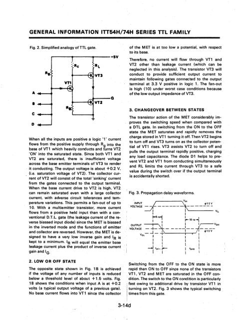
- Page 21 and 22: GENERAL INFORMATION ITT54/74 SERIES
- Page 23 and 24: GENERAL INFORMATION ITT54/74 SERIES
- Page 25 and 26: APPLICATION DATA FOR OPEN COLLECTOR
- Page 27 and 28: APPLICATION DATA FOR OPEN COLLECTOR
- Page 29: GENERAL INFORMATION ITT54/74 SERIES
- Page 33 and 34: ITT5400, ITT7400 QUADRUPLE 2-INPUT
- Page 35 and 36: ITT5401, ITT7401 QUADRUPLE 2-INPUT
- Page 37 and 38: ITT5402, .ITT7402 QUADRUPLE 2-INPUT
- Page 39 and 40: ITT5403, ITT7403 QUADRUPLE 2-INPUT
- Page 41 and 42: ITT5404,ITT7404 HEX INVERTERS ELECT
- Page 43 and 44: I TT540 5, ITT7405 HEX INVERTERS (W
- Page 45 and 46: ITT5406, ITT5416, ITT7406, ITT7416
- Page 47 and 48: _ I mm ..L..L. ___ SEMICONDUCTORS I
- Page 49 and 50: ITT ITT5408, ITT5409, ITT7408, ITT7
- Page 51 and 52: ITT5408,ITT5409, ITT7408, ITT7409 Q
- Page 53 and 54: ITT541 0, ITT741 0 TRIPLE 3-INPUT P
- Page 55 and 56: 0 10l ITT5411.ITT7411 TRIPLE 3-INPU
- Page 57 and 58: ITT5412, ITT7412 TRIPLE 3-INPUT POS
- Page 59 and 60: ITT5413,ITT7413 DUAL NAND SCHMITT T
- Page 61 and 62: ITT5420, ITT7420 DUAL 4-INPUT POSIT
- Page 63 and 64: ITI5421, ITT7421 DUAL 4-INPUT POSIT
- Page 65 and 66: ITT5425, ITT7425 DUAL 4-INPUT NOR G
- Page 67 and 68: ITT5426, ITT7426 QUADRUPLE 2-INPUT
- Page 69 and 70: ITT5428, ITT7428, ITT5433, ITT7433
- Page 71 and 72: ITT ITT5430, ITT7430 8-INPUT POSITI
- Page 73 and 74: ITT ITT5432, ITT7432 QUADRUPLE 2-IN
- Page 75 and 76: ITT ITT5437, ITT5438, ITT7437, ITT7
- Page 77 and 78: ITT5437, ITT5438, ITT7437, ITT7438
- Page 79 and 80: ITT5440, ITT7440 DUAL 4-INPUT POSIT
- Page 81 and 82:
ITT5442, ITT5443, ITT5444, ITT7442,
- Page 83 and 84:
w I Ol Ol INPUT! INMC OVTP\JT 0 OUT
- Page 85 and 86:
ITT5445, ITT54145, ITT7445, ITT7414
- Page 87 and 88:
ITT5445, ITT54145, ITT7445, ITT7414
- Page 89 and 90:
ITT5446A, ITT5447 A, ITT5448 ITT744
- Page 91 and 92:
ITT5446A, ITT5447 A, ITT5448 ITT744
- Page 93 and 94:
I TT5446A , ITT5447 A, ITT5448 ITT7
- Page 95 and 96:
ITT5446A, ITT5447 A, ITT5448 ITT744
- Page 97 and 98:
ITT5446A, ITT544 7 A, ITT5448 ITT74
- Page 99 and 100:
ITT5450, ITT5451 , IIT74!iO, 1T[745
- Page 101 and 102:
ITT . EXPANDABLE 4-WIDE 2-INPUT AND
- Page 103 and 104:
ITT5453. ITT5454. ITT7453. ITT7454
- Page 105 and 106:
ITT5460 , ITT7460 DUAL 4-INPUT'EXPA
- Page 107 and 108:
_ITT ________ E_D SEMICONDUCTORS ED
- Page 109 and 110:
ITT5470, ITT7470 EDGE-TRIGGERED J-K
- Page 111 and 112:
ITT5472, ITT7472 J-K MASTER-SLAVE F
- Page 113 and 114:
ITT ITT5473, ITT54107, ITT7473, ITT
- Page 115 and 116:
ITT5473, ITT54107, ITT7473, ITT7410
- Page 117 and 118:
ITT5474, ITT7474 DUAL D-TYPE EDGE-T
- Page 119 and 120:
I mm _".1-.1-___________ , SEMICOND
- Page 121 and 122:
ITT5475, ITT7475 • 4-BIT BISTABLE
- Page 123 and 124:
ITT ITT5476, ITT7476 DUALJ-K MASTER
- Page 125 and 126:
ITT5476, ITT7476 DUAL J-K MASTER-SL
- Page 127 and 128:
TYPES lTI5480, ITT7480 GATED FULL A
- Page 129 and 130:
TYPES ITT5480, ITT7480 GATED FULLAD
- Page 131 and 132:
ITT5482, ITT7482 2-BIT BINARY FULL
- Page 133 and 134:
ITT ITT5483, ITT7483 4-BIT BINARY F
- Page 135 and 136:
I TT5483 , ITT7483 4-BIT BINA RY FU
- Page 137 and 138:
ITT ITT5486, ITT7486 QUADRUPLE 2-IN
- Page 139 and 140:
__ JI[~~ __________________________
- Page 141 and 142:
ITT5490, ITT7490 DECADE COUNTERS EL
- Page 143 and 144:
ITT ITT5491A, ITT7491A 8-BIT SHIFT
- Page 145 and 146:
ITT5491 A, ITT7491 A 8-BIT SHIFT RE
- Page 147 and 148:
ITT5492, ITT7492 DIVIDE-BY-TWELVE C
- Page 149 and 150:
_. ITT ______________ 4-BIT BINARY
- Page 151 and 152:
ITT5493, ITT7493 4-BIT BINARY COUNT
- Page 153 and 154:
ITT5494, ITT7494 4-81T SHIFTREGISTE
- Page 155 and 156:
ITT ITT5495A, ITT7495A . 4-BIT RIGH
- Page 157 and 158:
ITT5495A. ITT7495A 4-811 RIGHT-SHIF
- Page 159 and 160:
:.:, ITT5496, ITT7496 5-BIT SHIFT R
- Page 161 and 162:
ITT 64104,74104,64106,74106,64109,7
- Page 163 and 164:
ITT54118, ITT74118 HEXSET-R~SET LAT
- Page 165 and 166:
ITT54121,ITT74121 MONOSTABLE MULTIV
- Page 167 and 168:
ITT54121,ITT74121 MONOSTABLE MULTIV
- Page 169 and 170:
ITT54121,ITT74121 MONOSTABLE MULTIV
- Page 171 and 172:
ITT54122, ITT54123, ITT74122, ITT74
- Page 173 and 174:
ITT54122, ITT54123, ITT74122, ITT74
- Page 175 and 176:
~ ITT _________ U_N_'V_E SEMICONDUC
- Page 177 and 178:
ITT74124 UNIVERSAL PULSE GENERATOR
- Page 179 and 180:
SWITCHING CHARACTERISTICS. Vee = 5V
- Page 181 and 182:
· ITT74124 UNIVERSAL PULSE GENERAT
- Page 183 and 184:
ITT54130, ITT74130, ITT54131, ITT74
- Page 185 and 186:
ITT54135, ITT54137, ITT74135, ITT74
- Page 187 and 188:
ITT ITT54138, ITT74138, ITT54139, I
- Page 189 and 190:
ITT ITT74141 BCD-TO-DECI MAL D ECOD
- Page 191 and 192:
ITT74141 BCD-TO-DECIMAL DECODER/DRI
- Page 193 and 194:
ITT54150, ITT54151, ITT74150, ITT74
- Page 195 and 196:
ITI54150, ITt54151, ITT74150, ITT74
- Page 197 and 198:
ITT54150, ITT54151, ITT74150, ITT74
- Page 199 and 200:
ITT54153, ITT74153 _ DUAL4-UNE-TO-1
- Page 201 and 202:
ITT54153,ITT74153 DUAL 4-UNE-TO-1-U
- Page 203 and 204:
ITT54154,ITT74154 4-LlN E-TO-16-LlN
- Page 205 and 206:
ITT ITT54155, ITT54156, ITT74155, I
- Page 207 and 208:
ITT54155, ITT54156, ITT74155, ITT74
- Page 209 and 210:
ITT54155, ITT54156, ITT74155, ITT74
- Page 211 and 212:
ITT54157, ITT74157 Quadruple 2-Line
- Page 213 and 214:
I mm -___L_L ________________ SEMIC
- Page 215 and 216:
ITT54160 THRU ITT54163, ITT74160THR
- Page 217 and 218:
ITT54160 THRU ITT54163,ITT74160THRU
- Page 219 and 220:
_ I mm ,ITT54164, ITT74164 .L.L ___
- Page 221 and 222:
ITT54164, ITT74164 8-BIT PARALLEL-O
- Page 223 and 224:
ITT54165, ITT74165 PARALLEL-LOAD 8-
- Page 225 and 226:
ITT ITT74174, ITT74175 HEX/QUADRUPL
- Page 227 and 228:
ITT74174, ITT74175 HEX/QUADRUPLE D-
- Page 229 and 230:
ITT54180,ITT74180 8-BIT ODD/EVEN PA
- Page 231 and 232:
ITT· ARITHMETIC SEMICONDUCTORS ITT
- Page 233 and 234:
ITT54181.ITT74181 ARITHMETIC LOGIC
- Page 235 and 236:
ITT54181, ITT.74181 ARJTHMETIC LOGI
- Page 237 and 238:
ITT54181, ITT74181 ARITHMETIC LOGIC
- Page 239 and 240:
ITT54182, ITT74182 LOOK-AHEAD CARRY
- Page 241 and 242:
IIT54182, IIT74182 LOOK-AHEAD CARRY
- Page 243 and 244:
ITT54190, ITT54191, ITT74190, ITT74
- Page 245 and 246:
ITT54190, ITT54191, ITT74190, ITT74
- Page 247 and 248:
ITT54190, ITI54191, ITT74190, ITT74
- Page 249 and 250:
I mm ..I....L ITT54/74192,ITT54/741
- Page 251 and 252:
ITT54/74192, ITT54/74193 SYNCHRONOU
- Page 253 and 254:
ITT54/74192,ITT54/74193 SYNCHRONOUS
- Page 255 and 256:
ITT 4-BIT SEMICONDUCTORS ITT54194,
- Page 257 and 258:
ITT54194, ITT74194 4-BIT BIDIRECTIO
- Page 259 and 260:
ITT ITT54195, ITT74195 4-81T PARALL
- Page 261 and 262:
ITT54195, ITT74195 4-81T PARALLEL-A
- Page 263 and 264:
ITT ITT54HOO, ITT74HOO QUADRUPLE 2-
- Page 265 and 266:
ITT CIRCUIT TYPES ITT54H01, ITT74H0
- Page 267 and 268:
ITT - ----- SEMICONDUCTORS HEX INVE
- Page 269 and 270:
_ I mm ITT54H05,ITT74H05 .L.L ____
- Page 271 and 272:
ITT CIRCUIT TYPES ITT54H10, ITT74H1
- Page 273 and 274:
ITT ITT54H11,ITT74H11 TRIPLE 3-INPU
- Page 275 and 276:
I mm CIRCUIT TYPES ITT54H20, ITT74H
- Page 277 and 278:
_ I mm CIRCUIT TYPES ITT54H21, ITT7
- Page 279 and 280:
_ I mm CIRCUIT TYPES ITT54H30, ITT7
- Page 281 and 282:
_ ITT _______ D_U_A_L_4_-_1 SEMICON
- Page 283 and 284:
ITT ITT54H50. ITT54H51. ITT74H50. I
- Page 285 and 286:
ITT54H50, ITT54:H51, ITT74H50, ITT7
- Page 287 and 288:
ITT54H53, ITT54H54, ITT74H53, ITT74
- Page 289 and 290:
ITT ITT54H60 DUAL4-INPUT EXPANDER (
- Page 291 and 292:
ITT ITT54H72, ITT74H72 __ .________
- Page 293 and 294:
ITT54H72, ITT74H72 J-K MASTER-SLAVE
- Page 295 and 296:
CIRCUIT TYPESITT54H73, ITT74H73 DUA
- Page 297 and 298:
ITT CIRCUIT TYPES ITT54H74, ITT74H7
- Page 299 and 300:
CIRCUIT TYPES ITT54H74, ITT74H74 DU
- Page 301 and 302:
ITT54H76, ITT74H76 DUALJ-K MASTER-S
- Page 303 and 304:
Series ITT9000-1, ITT9000-5 _][~~ _
- Page 305 and 306:
Series ITT9000-1, ITT9000-5 HIGH SP
- Page 307 and 308:
Ipd TEST CIRCUIT Vee 2.0 kll Series
- Page 309 and 310:
I TYPICAL INPUT AND OUTPUT CHARACTE
- Page 311 and 312:
Series ITT9000-1, 1119000-5 HIGH SP
- Page 313 and 314:
Series ITT9000-1, ITT9000-5 HIGH SP
- Page 315 and 316:
Series ITT9000-1, ITT9000-5 HIGH SP
- Page 317 and 318:
Series ITT9000-1, ITT9000-5 HIGH SP
- Page 319 and 320:
Series 11T9000-1, 1119000-5 HIGH SP
- Page 321 and 322:
Series ITT9000-1, ITT9000-5 HIGH SP
- Page 323 and 324:
Series ITT9000-1, ITT9000-5 HIGH SP
- Page 325 and 326:
ITT 9024 DUAL JK (OR D) FLIP-FLOP "
- Page 327 and 328:
ITT 9024 DUAL JK (OR D) FLIP-FLOP S
- Page 329 and 330:
ITT9300 MSI 4-Bit Shift Register 4.
- Page 331 and 332:
ITT9300 MSI A-Bit Sh ift Reg ister
- Page 333 and 334:
ITT9300 MSI 4-Bit Shift Register SE
- Page 335 and 336:
ITT9301 MSI One-Of-Ten Decoder ELEC
- Page 337 and 338:
1119301 MSI One-Of-Ten Decoder BCD
- Page 339 and 340:
ITT9304 MSI Dual Full Adder ELECTRI
- Page 341 and 342:
ITT9304 MSI Dual Full Adder LOW STA
- Page 343 and 344:
ITT9304 MSI Dual Full Adder GND c.>
- Page 345 and 346:
1119308 MSI Dual Four-Bit Latch ELE
- Page 347 and 348:
ITT9308 MSI Dual Four-Bit Latch CLO
- Page 349 and 350:
ITT9309 MSI Dual Four-Input Multipl
- Page 351 and 352:
ITT9309 MSI Dual Four-Input Multipl
- Page 353 and 354:
ITT9309 MSI Dual Four-Input Multipl
- Page 355 and 356:
ITT9309 MSI Dual Four-Input Multipl
- Page 357 and 358:
ITT9311 Msi One-Of-Sixteen Decoder
- Page 359 and 360:
ITT9311 Msi One-Of-Sixteen Decoder
- Page 361 and 362:
ITT9312 MSI Eight-Input Multiplexer
- Page 363 and 364:
ITT9312 MSI Eight-Input Multiplexer
- Page 365 and 366:
ITT9312 MSI Eight-Input Multiplexer
- Page 367 and 368:
ITT9316 MSI 4-Bit Binary Counter LO
- Page 369 and 370:
ITT9316 MSI 4-Bit Binary Counter CP
- Page 371 and 372:
ITT9322 Quad Two-Input Multiplexer
- Page 373 and 374:
ITT9322 Quad Two-Input Multiplexer
- Page 375 and 376:
ITT9328 MSI Dual 8-Bit Shift Regist
- Page 377 and 378:
ITT9328 MSI Dual 8-Bit Shift Regist
- Page 379 and 380:
ITT9601 Retriggerable Monostable Mu
- Page 381 and 382:
ITT9601 Retriggerable Monostable Mu
- Page 383 and 384:
ITT9601 Retriggerable Monostable Mu
- Page 385 and 386:
1... . .~ ITT9602 Dual Retriggerabl
- Page 387 and 388:
ITT9602 Dual Retriggerable Resettab
- Page 389 and 390:
ITT9602· Dual Retriggerable Resett
- Page 392 and 393:
ITT DTLDUAL FOUR-INPUT GATE FAST DT
- Page 394 and 395:
DTL DUAL FOUR-INPUT GATE ITT930 FAS
- Page 396 and 397:
ITT932, DUAL FOUR-INPUT BUFFER ITT9
- Page 398 and 399:
ITT932, DUALFOUR-INPUT BUFFER ITT94
- Page 400 and 401:
ITT EXTENDABLE HEX INVERTER ITT935,
- Page 402 and 403:
EXTENDABLE HEX INVERTER ITT935 HEX
- Page 404 and 405:
----______ 0. EXTENDABLE HEX INVERT
- Page 406 and 407:
ITT941, ITT951 MONOSTABLE MULTIVIBR
- Page 408 and 409:
ITT945,ITT948 c=:I[~~ _____________
- Page 410 and 411:
ITT945, ITT948 CLOCKED FLIP-FLOPS E
- Page 412 and 413:
ITT946 QUAD TWO-INPUT GATE ITT949 F
- Page 414 and 415:
ITT TRIPLETHREE-INPUTGATE ITT962 FA
- Page 416 and 417:
TRIPLE TH REE-INPUT GATE ITT962 FAS
- Page 418 and 419:
ITT1800 DTL DUAL FIVE INPUT Gate EL
- Page 420 and 421:
DTL QUAD TWO-INPUT AND GATE FAST DT
- Page 422 and 423:
I· _ oaI..oaI.. m.. m _____ FAST D
- Page 424 and 425:
DTL QUAD TWO-INPUT OR GATE FAST DTL
- Page 426 and 427:
ITT1810 ITT1811 DTL QUAD TWO-INPUT
- Page 428 and 429:
ITT ITT9093, ITT9094, ITT9097, ITT9
- Page 430 and 431:
ITT9093, ITT9094, ITT9097, ITT9099
- Page 432 and 433:
ITT9093, ITT9094, ITT9097, ITT9099
- Page 434 and 435:
_ I mm -IL-IL _____________ SEMICON
- Page 436 and 437:
ITT ITT302, ITT302H QUAD 2-INPUT (2
- Page 438 and 439:
...... 1 m .. T ___________ ITT303.
- Page 440 and 441:
_ I mm ITT311, ITT311 H MASTER SLAV
- Page 442 and 443:
ITT311, ITT311 H MASTER SLAVE FLIP-
- Page 444 and 445:
ITT312, ITT312H DUAL J-K FLIP-FLOP
- Page 446 and 447:
ITT ITT321, ITT321 H QUAD 2-INPUT (
- Page 448 and 449:
ITT ITT322, ITT322H DUAL 5-INPUT EX
- Page 450 and 451:
ITT ITT323, ITT323H QUAD 2-INPUT (2
- Page 452 and 453:
_ IT m ITT324, ITT324H QUAD 2-INPUT
- Page 454 and 455:
ITT ITT325, ITT325H ....... .___ D_
- Page 456 and 457:
ITT ITT326, ITT326H DUAL 2, DUAL 3-
- Page 458 and 459:
I mm ITT331, ITT331 H DUAL 5-INPUT
- Page 460 and 461:
ITT332, ITT332H QUAD INVERTER, DUAL
- Page 462 and 463:
ITT333, ITT333H QUAD INVERTER, DUAL
- Page 464 and 465:
ITT334, ITT334H STROBED HEX INVERTE
- Page 466 and 467:
ITT335, ITT335H STROBED HEX INVERTE
- Page 468 and 469:
ITT342 , ITT342H DUAL MONOST ABLE M
- Page 470 and 471:
ITT343, ITT343H FOUR-BIT COMPARATOR
- Page 472 and 473:
ITT ITT361, ITT361H DUAL HIGH TO LO
- Page 474 and 475:
ITT361, ITT361 H DUAL HIGH TO LOW I
- Page 476 and 477:
ITT362, ITT362H DUAL LOW TO HIGH IN
- Page 478 and 479:
ITT ITT370, ITT370H QUAD D FLIP-FLO
- Page 480 and 481:
ITT ITT371, ITT371 H DECADE COUNTER
- Page 482 and 483:
ITT371, ITT371 H DECADE COUNTER ELE
- Page 484 and 485:
ITT372, ITT372H DIVIDE BY 16 (HEXAD
- Page 486 and 487:
ITT372, ITT372H DIVIDE BY 16 (HEXAD
- Page 488 and 489:
ITT380, ITT381, ITT380H, ITT381 H B
- Page 490 and 491:
_ I mm ITT7520 SENSE AMPLIFIERS -L-
- Page 492 and 493:
ITT7520 SENSE AMPLIFIERS The logic
- Page 494 and 495:
ITT7520 SENSE AMPLIFIERS Sense-inpu
- Page 496 and 497:
ITT7520, ITT7521 DUAL-CHANNEL SENSE
- Page 498 and 499:
ITT ITT7522, ITT7523 DUAL-CHANNEL S
- Page 500 and 501:
ITT7522, ITT7523 DUAL-CHANNEL SENSE
- Page 502 and 503:
ITT7524, ITT7525 DUAL SENSE AM PLiF
- Page 504 and 505:
_ I ITT7528, ITT7529 rI1m _____ D_U
- Page 506 and 507:
ITT7528, ITT7529 DUAL SENSE AMPLIFI
- Page 508 and 509:
ITT5534/1TT7534 and ITT5535/1TT7535
- Page 510 and 511:
ITT5534/1TT7534 and ITT5535/1TT7535
- Page 512 and 513:
ITT75234, ITT75235 DUAL SENSE AMPLI
- Page 514 and 515:
ITT ITT7520 SENSE AMPLIFIERS - ----
- Page 516 and 517:
ITT7520 SENSE AM PLiFIERS PARAMETER
- Page 518 and 519:
ITT7520 SENSE AMPLIFIERS PARAMETER
- Page 520 and 521:
ITT7520 SENSE AM PLiFIERS PARAMETER
- Page 522 and 523:
ITT7520 SENSE AMPLIFIERS PARAMETER
- Page 524 and 525:
ITT7520 SENSE AMPLIFIERS PARAMETER
- Page 526 and 527:
ITT7520 SENSE AMPLIFIERS PARAMETER
- Page 528 and 529:
11T7520 SENSE AM PLiFIERS PARAMETER
- Page 530 and 531:
ITT7520 SENSE AM PLIFIERS PARAMETER
- Page 532 and 533:
ITT7520 SENSE AMPLIFIERS PARAMETER
- Page 534 and 535:
ITT7520 SENSE AMPLIFIERS TYPICAL CH
- Page 536 and 537:
ITT7520 SENSE AMPLIFIERS Large Memo
- Page 538 and 539:
ITT3671 HIGH-SPEED DUAL SENSE AMPLI
- Page 540 and 541:
ITT3671 HIGH-SPEED DUAL SENSE AMPLI
- Page 542 and 543:
ITT3671 HIGH-SPEED DUAL SENSE AMPLI
- Page 544 and 545:
ITT3671 HIGH-SPEED DUAL SENSE AMPLI
- Page 546 and 547:
ITT3671 HIGH-SPEED DUAL SENSE AMPLI
- Page 548 and 549:
ITT3671 HIGH-SPEED DUAL SENSE AMPLI
- Page 550 and 551:
ITT3671 HIGH-SPEED DUAL SENSE AMPLI
- Page 552 and 553:
I ..L.L rIlrll ITT9614 DUAL DIFFERE
- Page 554 and 555:
ITT9614 DUAL DIFFERENTIAL LINE DRIV
- Page 556 and 557:
ITT9614 DUAL DIFFERENTIAL LINE DRIV
- Page 558 and 559:
_ I mm ITT9615 DUAL DIFFERENTIAL LI
- Page 560 and 561:
ITT9615 DUAL DIFFERENTIAL LINE RECE
- Page 562 and 563:
ITT9615 DUAL DIFFERENTIAL LINE RECE
- Page 564 and 565:
_ I mm. ______________ ~~ MEMORY DR
- Page 566 and 567:
ITT75324 MEMORY DRIVER WITH DECODE
- Page 568 and 569:
ITT75324 MEMORY DRIVER WITH DECODE
- Page 570 and 571:
ITT ITT709 I ITT709-A HIGH PERFORMA
- Page 572 and 573:
ITT709, ITT709-A HIGH PERFORMANCE O
- Page 574 and 575:
ITT709 I ITT709-A HIGH PERFORMANCE
- Page 576 and 577:
ITT709, ITT709-A HIGH PERFORMANCE O
- Page 578 and 579:
ITT ITT710 HIGH SPEED DIFFERENTIAL
- Page 580 and 581:
ITT710 HIGH SPEED DIFFERENTIAL COMP
- Page 582 and 583:
~TT710 HIGH SPEED DIFFERENTIAL COMP
- Page 584 and 585:
ITT710 HIGH SPEED DIFFERENTIAL COMP
- Page 586 and 587:
ITT ITT711 DUAL COMPARATOR - -----
- Page 588 and 589:
ITT711 DUAL COMPARATOR Schematic Di
- Page 590 and 591:
!TT711 DUAL COMPARATOR OUTPUT SINK
- Page 592 and 593:
_ I mm ITT712 HIGH-GAIN WIDEBAND DC
- Page 594 and 595:
----~-- ITT712 HIGH-GAIN WIDEBAND D
- Page 596 and 597:
ITT712 HIGH-GAIN WIDEBAND DC AMPLIF
- Page 598 and 599:
ITT712 HIGH-GAIN WIDEBAND DC AMPLIF
- Page 600 and 601:
_____ ITT712 HIGH-GAIN WIDEBAND DC
- Page 602 and 603:
ITT720 DUAL HIGH SPEED DIFFERENTIAL
- Page 604 and 605:
ITT720 DUAL HIGH SPEED DIFFERENTIAL
- Page 606 and 607:
ITT720 DUAL HIGH SPEED DIFFERENTIAL
- Page 608 and 609:
ITT 723 PRECISION VOLTAGE REGULATOR
- Page 610 and 611:
ITT723 PRECISION VOLTAGE REGULATOR
- Page 612 and 613:
ITT723 PRECISION VOLTAGE REGULATOR
- Page 614 and 615:
ITT723 PRECISION VOLTAGE REGULATOR
- Page 616 and 617:
ITT ITT726 TEMPERATURE-CONTROLLED D
- Page 618 and 619:
ITT726 TEMPERATURE-CONTROLLED DIFFE
- Page 620 and 621:
ITT ITT741 HIGH PERFORMANCE OPERATI
- Page 622 and 623:
ITT741 HIGH PERFORMANCE OPERATIONAL
- Page 624 and 625:
ITT741 HIGH PERFORMANCE OPERATIONAL
- Page 626:
ITT741 HIGH PERFORMANCE OPERATIONAL
- Page 629 and 630:
ITT491, ITT492 MOS TO LED SEGMENT A
- Page 631 and 632:
ITT 491, ITT 492 MOS TO LED SEGMENT
- Page 633 and 634:
ITT ITT501 QUAD SEGMENT DRIVER - --
- Page 635 and 636:
ITT 11T502 HEX DIGIT DRIVER - -----
- Page 637 and 638:
ITT ITT503 QUAD SEGMENT DRIVER - --
- Page 639 and 640:
_' Imm _________ -L-L 'T_Ts_os GAS
- Page 641 and 642:
_ I mm ITT508 OCTAL DIGIT DRIVER .1
- Page 643 and 644:
I mm _ . .L.L _______ O_C_T_A SEMIC
- Page 645 and 646:
_ I mm ITT7103 .L-L ____ _ SEMICOND
- Page 647 and 648:
_ I mm ITT7105 EIGHT DIGIT DRIVER .
- Page 649 and 650:
_ . ITT SEMICONDUCTORS TBA940 HORIZ
- Page 651 and 652:
TBA940 HORIZONTAL DEFLECTION PROCES
- Page 653 and 654:
_ I mm JLJL ________ P_R_O_C_E_S_80
- Page 655 and 656:
68k r- 20ms 1 :V~ram. pull .. I I I
- Page 657 and 658:
ITT TBA120S INTEGRATED FM/IF AMPLIF
- Page 659 and 660:
TBA120S INTEGRATED FM/IF AMPLIFIER
- Page 661 and 662:
TBA120S INTEGRATED FM/IF AMPLIFIER
- Page 663 and 664:
ITT3064 TV AUTOMATIC FINE-TUNING CI
- Page 665 and 666:
ITT3064 TV AUTOMA TIC FINE-TUNING C
- Page 667 and 668:
ITT~65 TV IFM SOUND SYSTEM TYPICAL
- Page 669 and 670:
ITT3065 TV IFM SOUNDSYSTEM IF AMPLI
- Page 671 and 672:
TDA1330 LOW~LEVEL VIDEO DETECTOR .
- Page 673 and 674:
I mm _-IL-IL _____ SEMICONDUCTORS T
- Page 675 and 676:
TDA1352 TV VIDEO IF AMPLIFIER WITH
- Page 677 and 678:
_ ITT ______ 2_W_A_T_T_T_V_S_O ....
- Page 679 and 680:
ITT3701 2 WAn TV SOUND SYSTEM Fig.
- Page 681 and 682:
_ I mm ITT SAJ110 SEVEN STAGE FREQU
- Page 683 and 684:
ITT SAJ110 FREQUENCY DIVIDER CIRCUI
- Page 685 and 686:
ITT SAJ110 FREQUENCY DIVIDER CIRCUI
- Page 687 and 688:
ITT SAJ110 FREQUENCY DIVIDER CIRCUI
- Page 689 and 690:
SAH190 MaS TONE GENERATOR CHARACTER
- Page 691 and 692:
SAH190 MOS TONE GENERATOR are fed t
- Page 693 and 694:
SAH190 MOS TONE GENERATOR Table 1:
- Page 695 and 696:
SAH190 MOS TONE GENERATOR be connec
- Page 697 and 698:
ITT ITT TBA800 5 WATT AUDIO AMPLIFI
- Page 699 and 700:
TBA800 5 WATT AUDIO AMPLIFIER '/. 5
- Page 701 and 702:
_ ITT ________ SEMICONDUCTORS TCA25
- Page 703 and 704:
TCA250 DUAL FILTER AMPLIFIER Circui
- Page 705 and 706:
TCA270 SYNCHRONOUS DEMODULATOR AGC
- Page 707 and 708:
TCA350 ANALOG SHIFT REGISTER (OELA
- Page 709 and 710:
ZTK6.8 to ZTK33 (TAA550) MONOLITHIC
- Page 711 and 712:
ZTK6.8 to ZTK33 (TAA550) MONOLITHIC
- Page 713 and 714:
ZTKS.8 to ZTK33 (TAA550) MONOLITHIC
- Page 715 and 716:
ZTK33DPD MONOLITHIC TEMPERATURE . C
- Page 717 and 718:
UAA110 CAMERA INTEGRATED CIRCUIT Al
- Page 719 and 720:
UAA110 CAMERA INTEGRATED CIRCUIT v
- Page 721 and 722:
SAJ220 FAMILY QUARTZ WATCH & CLOCK
- Page 723 and 724:
TAA780 1.tV STABILIZING CIRCUIT CHA
- Page 725 and 726:
____ TBA840, TCA840 WRIST-WATCH BAL
- Page 727 and 728:
_ I mm TAA775G POWER OSCILLATOR ..L
- Page 729 and 730:
TAA775G POWER OSCILLATOR Dynamic Ch
- Page 731 and 732:
_ ITT ___ SEMICONDUCTORS SAK115 T_A
- Page 733 and 734:
I mm SAY115 SPEEDOMETER INTEGRATED
- Page 736 and 737:
_ I mm -L..L_____ SEMICONDUCTORS SM
- Page 738 and 739:
ITT MPS-A05 NPN SI LICON AUDIO TRAN
- Page 740 and 741:
__ I mm _L_L ___________ N_P_N SEMI
- Page 742 and 743:
ITT MPS-A70 GENERAL PURPOSE PNP SI
- Page 744 and 745:
ITT MPS834 HIGH-SPEED NPN SILICON S
- Page 746 and 747:
ITT MPS2711, MPS2712 LOW-POWER NPN
- Page 748 and 749:
Package: T 0-92 MPS2923 THRU MPS292
- Page 750 and 751:
ITT MPS3392 thru MPS3395 NPN SILICO
- Page 752 and 753:
MPS3638, MPS3638A ELECTRICAL CHARAC
- Page 754 and 755:
MPS3702, MPS3703 LOW-POWER PNP SILI
- Page 756 and 757:
ITT MPS3707 thru MPS3711 GENERAL PU
- Page 758 and 759:
MPS6530 thru MPS6532 NPN SILICON AM
- Page 760 and 761:
Package: To-92 MPS6565, MPS6566 GEN
- Page 762 and 763:
ITT 2N696 SILICON GENERAL PURPOSE T
- Page 764 and 765:
2N706.2N706A.2N706B SILICON SWITCHI
- Page 766 and 767:
ITT 2N744 SILICON SWITCHING TRANSIS
- Page 768 and 769:
ITT 2N2195, 2N2195A, 2N2195B® HIGH
- Page 770 and 771:
2N929, 2N930 SILICON GENERAL PURPOS
- Page 772 and 773:
2N2217, 2N2218, 2N2219 SILICON GENE
- Page 774 and 775:
2N2219A SILICON SWITCHING TRANSISTO
- Page 776 and 777:
2N2221, 2N2222 SILICON GENERAL PURP
- Page 778 and 779:
2N2221A® ELECTRICAL CHARACTERISTIC
- Page 780 and 781:
2N2222A SILICON SWITCHING TRANSISTO
- Page 782 and 783:
2N2368, 2N2369 SILICON SWITCHING TR
- Page 784 and 785:
2N2368, 2N2369 SILICON SWITCHING TR
- Page 786 and 787:
ITT 2N2369A SILICON SWITCHING TRANS
- Page 788 and 789:
2N2369A SILICON SWITCHING TRANSISTO
- Page 790 and 791:
2N2369A SILICON SWITCHING TRANSISTO
- Page 792 and 793:
ITT 2N2480,2N2480A -- NPN SILICON D
- Page 794 and 795:
ITT 2N2483. 2N2484 SILICON GENERAL
- Page 796 and 797:
2N2483, 2N2484 SILICON GENERAL PURP
- Page 798 and 799:
2N2483, 2N2484 SILICON GENERAL PURP
- Page 800 and 801:
ITT 2N2904A, 2N2905A, 2N2906A., 2N2
- Page 802 and 803:
ITT 2N3011® HIGH-SPEED NPN SILICON
- Page 804 and 805:
ITT 2N3053 NPN SILICON SWITCHING AN
- Page 806 and 807:
2N3502,2N3503,2N3504,2N3505 ELECTRI
- Page 808 and 809:
ITT 2N3724, 2N3725, 2N4013, 2N4014
- Page 810 and 811:
2N3724, 2N3725, 2N4013, 2N4014 SILI
- Page 812 and 813:
2N3724, 2N3725, 2N4013, 2N4014 SILI
- Page 814 and 815:
2N3903, 2N3904 Package: TO-92 NPN S
- Page 816 and 817:
2N3903.2N3904 ELECTRICAL CHARACTERI
- Page 818 and 819:
2N3905,2N3906 ELECTRICAL CHARACTERI
- Page 820 and 821:
2N3962,2N3963,2N3964,2N396S® PNP S
- Page 822 and 823:
2N3962,2N3963,2N3964,2N3965 ELECTRI
- Page 824 and 825:
Package: To-92 2N4125,2N4126. GENER
- Page 826 and 827:
2N4248,2N4249,2N4250 ELECTRICAL CHA
- Page 828 and 829:
Package: To-92 2N4400, 2N4401 GENER
- Page 830 and 831:
2N4402, 2N4403· GENERAL PURPOSE PN
- Page 832 and 833:
Package: To-92 2N4418,2N4419 LOW·L
- Page 834 and 835:
Package: To-92 2N4420, 2N4421, 2N44
- Page 836 and 837:
Package: To-92 2N5086, 2N5087 LOW-L
- Page 838 and 839:
Package: To-92 2N5209, 2N5210 LOW-L
- Page 840 and 841:
Package: To-92 ··2N5220. LOW-POWE
- Page 842 and 843:
2N5223 Package: To-92 LOW-LEVEL GEN
- Page 844 and 845:
Package: To-92 2N5225 MEDIUM POWER
- Page 846 and 847:
Package: To-92 2N5227 GENERAL PURPO
- Page 848 and 849:
2N5368 thru 2N537.1 GENERAL PURPOSE
- Page 850 and 851:
Package: TO- 92 2N5376, .2N5377 GEN
- Page 852 and 853:
2N5378,2N5379 GENERAL PURPOSE PNP S
- Page 854:
2N5449,2N5450,2N5451 NPNSILICON AMP
- Page 857 and 858:
GOLD BOND GERMANIUM DIODES Part No.
- Page 859 and 860:
GOLD BOND GERMANIUM DIODES ELECTRIC
- Page 861 and 862:
GOLD BOND GERMANIUM DIODES _. - ELE
- Page 863 and 864:
GOLD BOND GERMANIUM DIODES ELECTRIC
- Page 865 and 866:
_ I mm -L-L ____ _ SEMICONDUCTORS S
- Page 867 and 868:
SILICON PLANAR DIODE ELECTRICAL CHA
- Page 869 and 870:
SILICON PLANAR DIODE ELECTRICAL CHA
- Page 871 and 872:
ITT JAN 1N4148 SILICON SWITCHING DI
- Page 873 and 874:
ITT ITT600 SILICON SWITCHING DIODE
- Page 875 and 876:
ITT ITT2001, ITT2002, ITT2003 SILIC
- Page 877 and 878:
_ I mm ITT3001, ITT3002, ITT3003 HI
- Page 879 and 880:
_ T 1 N5194, 1 N5195, 1 N5196 GENER
- Page 882 and 883:
ITT ----- SELENIUM CONTACT PROTECTO
- Page 884 and 885:
SELENIUM CONTACT PROTECTORS DC APPL
- Page 886 and 887:
SELENIUM CONTACT PROTECTORS Figure
- Page 888 and 889:
ITT SELENIUM TRANSIENT VOLTAGE SUPP
- Page 890 and 891:
TRANSIENT VOLTAGE SELENIUM SUPPRESS
- Page 892 and 893:
CHARACTERISTIC CURVES 130 - , 120 S
- Page 894 and 895:
_ I mm -L-L ______ SEMICONDUCTORS 1
- Page 896 and 897:
1 N4000 SERIES, EM500 SERIES PLASTI
- Page 898 and 899:
1 N4000 SERIES, EM500 SERIES -----.
- Page 900 and 901:
ITT 1 N4383/5, 1 N4585/6, RG1122/3
- Page 902 and 903:
1 N4383/5, 1 N4585/6, RG1122/3 1-AM
- Page 904 and 905:
ITT 1 N5400 THROUGH 1 N5408 SILICON
- Page 906 and 907:
_ I mm -1--1-_____ SEMICONDUCTORS E
- Page 908 and 909:
ENTERTAINMENT TYPE SELENIUM RECTIFI
- Page 910 and 911:
ENTERTAINMENT TYPE SELENIUM RECTIFI
- Page 912 and 913:
ITT 1N746 THROUGH 1N759 ZENER DIODE
- Page 914 and 915:
ITT IN957 THRU IN973 ZENER DIODES -
- Page 916 and 917:
_ I mm JLJL ____________________ SE
- Page 918 and 919:
1 N4729 THROUGH 1 N4752 ZENER DIODE
- Page 920 and 921:
1 N5226 THROUGH 1 N5257 ZENER DIODE
- Page 922 and 923:
ITT ITT-lOgE) TUNER DIODE - ----- S
- Page 924 and 925:
ITT ITT-141 ITT-142® TUNER DIODES
- Page 926 and 927:
ITT -141 ITT -142 TYPICAL CHARACTER
- Page 928 and 929:
_ITT________ AFC TUNER ITT_2_10 DIO
- Page 930 and 931:
m ~ liLT =====-= SEMICONDUCTORS ...
- Page 932 and 933:
TUNER DIODES V - SERIES .,' 1 8 6 5
- Page 934:
TUNER DIODES U - SERIES B CAPACITAN
- Page 937 and 938:
1N3831 THR-QUGH1N3846 ELECTRICAL CH
- Page 939 and 940:
TYPEE 4E20-4E200 ELECTRICAL CHARACT
- Page 941 and 942:
TYPE E4E20M· 4E200M ELECTRICAL CHA
- Page 943 and 944:
APPLICATION NOTES FOUR-LAYER DIODE
- Page 945 and 946:
APPLICATION NOTES FOUR-LAYER DIODE
- Page 947 and 948:
APPLICATION NOTES FOUR-LAYER DIODE
- Page 949 and 950:
APPLICATION NOTES FOUR-LAVER DIODE
- Page 951 and 952:
TYPE TAG . Plastiq Encapsulated Tan
- Page 953 and 954:
TYPE TAG Plastic Encapsulated Tanta
- Page 955 and 956:
ITT SEMICONDUCTORS TYPE TAP PLASTIC
- Page 957 and 958:
TYPE TAP PLASTIC ENCAPSULATED TANTA
- Page 959 and 960:
TYPE TAP PLASTIC ENCAPSULATED TANTA
- Page 961 and 962:
TYPE TAM Plastic Encapsulated Tanta
- Page 963 and 964:
TYPE TAM Plastic Encapsulated Tanta
- Page 965 and 966:
PACKAGE DIMENSIONS 16-Lead Ceramic
- Page 967 and 968:
PACKAGE DIMENSIONS DIMENSIONS - FLA
- Page 969 and 970:
PACKAGE DIMENSIONS PHYSICAL DIMENSI
- Page 972:
For Price and Delivery Information