- Page 1 and 2:
5 Simulation System SIMPLORER ® 6.
- Page 3:
Printing History SIMPLORER 6.0 —
- Page 7 and 8:
Table of Contents SIMPLORER 6.0 —
- Page 9 and 10:
SIMPLORER 6.0 — Manual ix 12.3 Vi
- Page 11 and 12:
General Description of Content SIMP
- Page 13 and 14:
1 Introduction SIMPLORER 6.0 — Ma
- Page 15 and 16:
Installing SIMPLORER Hardware and S
- Page 17 and 18:
2 Project Management SIMPLORER 6.0
- Page 19 and 20:
Opional Programs • Analytical Fre
- Page 21 and 22:
SIMPLORER 6.0 — Manual 9 The «Sh
- Page 23 and 24:
Starting SIMPLORER Programs SIMPLOR
- Page 25 and 26:
SSC Commander Icon on the Taskbar S
- Page 27 and 28:
Command Toolbar Symbol and Descript
- Page 29 and 30:
Sorting Criteria SIMPLORER 6.0 —
- Page 31 and 32:
Dialog Tab/Options Description Add
- Page 33 and 34:
Options Menu — Directories � Di
- Page 35 and 36:
Command Description The Options men
- Page 37 and 38:
2.7 Version’s Report and Online H
- Page 39 and 40:
3 General Modeling Functions SIMPLO
- Page 41 and 42:
SI Units SIMPLORER 6.0 — Manual 2
- Page 43 and 44:
Characteristic Type (Name.CH) File
- Page 45 and 46:
Logic operators (must be surrounded
- Page 47 and 48:
3.2 Schematic Operating Environment
- Page 49 and 50:
Schematic Sheet Model Tree Object B
- Page 51 and 52:
3.3 Creating Simulation Models Star
- Page 53 and 54:
Component Overview SIMPLORER 6.0
- Page 55 and 56:
Searching for Components SIMPLORER
- Page 57 and 58:
Displaying and Hiding Pins SIMPLORE
- Page 59 and 60:
SIMPLORER 6.0 — Manual 47 Place t
- Page 61 and 62:
Defining Parameters Fixed Component
- Page 63 and 64:
Defining Displays and Outputs SIMPL
- Page 65 and 66:
Using Simulation Parameters SIMPLOR
- Page 67 and 68:
3.4 Characteristics in Simulation M
- Page 69 and 70:
SIMPLORER 6.0 — Manual 57 Define
- Page 71 and 72:
5 The new pin symbol can now be con
- Page 73 and 74:
Transferring Parameter Values into
- Page 75 and 76:
SIMPLORER 6.0 — Manual 63 5 Defin
- Page 77 and 78:
3.6 Modifying Component Parameters
- Page 79 and 80:
SIMPLORER 6.0 — Manual 67 Search
- Page 81 and 82:
SIMPLORER 6.0 — Manual 69 If you
- Page 83 and 84:
4 Modeling with Circuit Components
- Page 85 and 86:
Component Outputs SIMPLORER 6.0 —
- Page 87 and 88:
Component Parameters SIMPLORER 6.0
- Page 89 and 90:
SIMPLORER 6.0 — Manual 77 «Initi
- Page 91 and 92:
Inductor SIMPLORER 6.0 — Manual 7
- Page 93 and 94:
Component Parameters SIMPLORER 6.0
- Page 95 and 96:
Component Outputs Mutual Inductance
- Page 97 and 98:
SIMPLORER 6.0 — Manual 85 � «T
- Page 99 and 100:
Component Outputs Controlled Voltag
- Page 101 and 102:
Current Source SIMPLORER 6.0 — Ma
- Page 103 and 104:
Component Outputs SIMPLORER 6.0 —
- Page 105 and 106:
SIMPLORER 6.0 — Manual 93 «Early
- Page 107 and 108:
Component Outputs Voltage Controlle
- Page 109 and 110:
Polynomial Source SIMPLORER 6.0 —
- Page 111 and 112:
Fourier Source SIMPLORER 6.0 — Ma
- Page 113 and 114:
SIMPLORER 6.0 — Manual 101 � «
- Page 115 and 116:
Power Source SIMPLORER 6.0 — Manu
- Page 117 and 118:
Ideal Transfer Switch SIMPLORER 6.0
- Page 119 and 120:
4.4 Semiconductors System Level Dio
- Page 121 and 122:
IGBT Component Outputs SIMPLORER 6.
- Page 123 and 124:
Component Outputs MOS Fieldeffect T
- Page 125 and 126:
Component Outputs Bipolar Junction
- Page 127 and 128:
Component Outputs GTO-Thyristor SIM
- Page 129 and 130:
Thyristor Component Outputs SIMPLOR
- Page 131 and 132:
TRIAC Component Outputs SIMPLORER 6
- Page 133 and 134:
Component Outputs SIMPLORER 6.0 —
- Page 135 and 136:
Electrical Behavior Level, Type DYN
- Page 137 and 138:
Irr[A] Irrmax i2 (sin) i1 (exp) �
- Page 139 and 140:
Dynamic IGBT Model SIMPLORER 6.0
- Page 141 and 142:
SIMPLORER 6.0 — Manual 129 There
- Page 143 and 144:
SIMPLORER 6.0 — Manual 131 Intern
- Page 145 and 146:
Electrical Behavior Level, Type DYN
- Page 147 and 148:
Dynamic FET Model SIMPLORER 6.0 —
- Page 149 and 150:
Component Parameters SIMPLORER 6.0
- Page 151 and 152:
Freewheeling Diode Model SIMPLORER
- Page 153 and 154:
Electrical Model SIMPLORER 6.0 —
- Page 155 and 156:
Electrical Behavior Level, Type DYN
- Page 157 and 158:
Component Nodes SIMPLORER 6.0 — M
- Page 159 and 160: SIMPLORER 6.0 — Manual 147 and Ca
- Page 161 and 162: SIMPLORER 6.0 — Manual 149 Elemen
- Page 163 and 164: 4.6 SPICE-Compatible Models • Dio
- Page 165 and 166: SIMPLORER 6.0 — Manual 153 specif
- Page 167 and 168: 4.6.2 Diode Models Diode SIMPLORER
- Page 169 and 170: Current and Voltage Reference Arrow
- Page 171 and 172: Current and Voltage Reference Arrow
- Page 173 and 174: SIMPLORER 6.0 — Manual 161 BSIM3
- Page 175 and 176: MESFET Model SIMPLORER 6.0 — Manu
- Page 177 and 178: SIMPLORER 6.0 — Manual 165 The in
- Page 179 and 180: 4.7 Electrical Machines • Inducti
- Page 181 and 182: SIMPLORER 6.0 — Manual 169 Initia
- Page 183 and 184: SIMPLORER 6.0 — Manual 171 Motion
- Page 185 and 186: Synchronous Machine Electrical Exci
- Page 187 and 188: SIMPLORER 6.0 — Manual 175 Initia
- Page 189 and 190: SIMPLORER 6.0 — Manual 177 Electr
- Page 191 and 192: Flux-linkage equations ψ1d() t = i
- Page 193 and 194: DC Machine Permanent Excitation SIM
- Page 195 and 196: DC Machine Linear Electrical Excita
- Page 197 and 198: DC Machine Nonlinear Electrical Exc
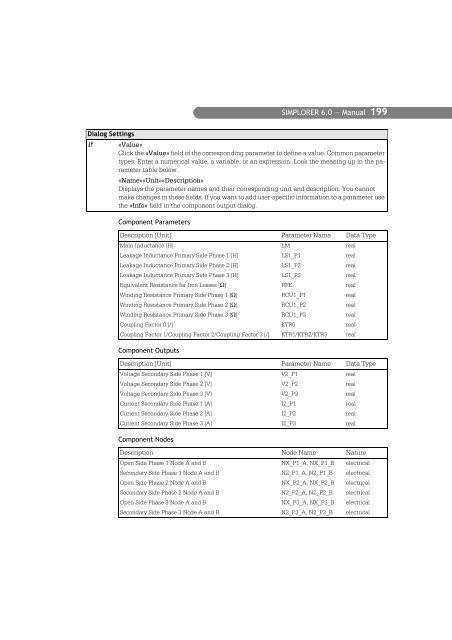
- Page 199 and 200: 4.8 Transformers • Single-Phase S
- Page 201 and 202: Linear Two-winding Transformer SIMP
- Page 203 and 204: Nonlinear Two-winding Transformer S
- Page 205 and 206: Component Parameters Secondary Side
- Page 207 and 208: W 2 KTR = ------- with W1 = Winding
- Page 209: W 2 KTR = ------- with W1 = Winding
- Page 213 and 214: 5 Modeling with Block Diagrams SIMP
- Page 215 and 216: Defining the Sample Time You can ch
- Page 217 and 218: Integrator SIMPLORER 6.0 — Manual
- Page 219 and 220: Component Parameters Derivative SIM
- Page 221 and 222: Component Outputs Dead-Time Element
- Page 223 and 224: 5.2 Discrete Blocks • Z-Transfer
- Page 225 and 226: Discrete Integrator SIMPLORER 6.0
- Page 227 and 228: 4 SIMPLORER 6.0 — Manual 215 Dial
- Page 229 and 230: SIMPLORER 6.0 — Manual 217 � «
- Page 231 and 232: Component Outputs Step Function SIM
- Page 233 and 234: Component Outputs 5.4 Signal Proces
- Page 235 and 236: Summation SIMPLORER 6.0 — Manual
- Page 237 and 238: Negator SIMPLORER 6.0 — Manual 22
- Page 239 and 240: Component Outputs Comparator >>Basi
- Page 241 and 242: Component Parameters N-Point Elemen
- Page 243 and 244: Nonlinear Transfer Function >>Basic
- Page 245 and 246: Maximum/Minimum Value at Time T SIM
- Page 247 and 248: SIMPLORER 6.0 — Manual 235 �
- Page 249 and 250: 5.5 Math • Sine (FCT) • Cosine
- Page 251 and 252: Root Sign SIMPLORER 6.0 — Manual
- Page 253 and 254: 6 Modeling with State Graphs SIMPLO
- Page 255 and 256: Differences in Assignment Actions i
- Page 257 and 258: Changing Action Types SIMPLORER 6.0
- Page 259 and 260: State Graph Components • Transiti
- Page 261 and 262:
7 Using Measuring Instruments SIMPL
- Page 263 and 264:
Magnetic Meters SIMPLORER 6.0 — M
- Page 265 and 266:
Velocity-Force-Representation—Rot
- Page 267 and 268:
8 Using Signal Characteristics SIMP
- Page 269 and 270:
Component Parameters Event Triggere
- Page 271 and 272:
8.2 Dynamic Behavior Parameters •
- Page 273 and 274:
Pulse Duration SIMPLORER 6.0 — Ma
- Page 275 and 276:
8.3 Dynamic Performance Parameters
- Page 277 and 278:
Overshoot Characteristics SIMPLORER
- Page 279 and 280:
Component Parameters 8.4 Special Wa
- Page 281 and 282:
Sliding Mean Value SIMPLORER 6.0
- Page 283 and 284:
Component Outputs Power and Energy
- Page 285 and 286:
SIMPLORER 6.0 — Manual 273 «Scan
- Page 287 and 288:
9 Modeling Tools SIMPLORER 6.0 —
- Page 289 and 290:
Sine Wave >>Basics>Tools>Time Funct
- Page 291 and 292:
Triangular Wave >>Basics>Tools>Time
- Page 293 and 294:
Trapezoidal Wave >>Basics>Tools>Tim
- Page 295 and 296:
SIMPLORER 6.0 — Manual 283 «Dela
- Page 297 and 298:
Needle Pulses SIMPLORER 6.0 — Man
- Page 299 and 300:
Component Outputs 2D Lookup Table S
- Page 301 and 302:
PWM Component Outputs SIMPLORER 6.0
- Page 303 and 304:
Equivalent Line SIMPLORER 6.0 — M
- Page 305 and 306:
⎛ VT ⎞ qt () = ( TAU ⋅ ISAT)
- Page 307 and 308:
2D Lookup Table XY SIMPLORER 6.0
- Page 309 and 310:
Separate Component Characteristic S
- Page 311 and 312:
SIMPLORER 6.0 — Manual 299 � «
- Page 313 and 314:
Equations SIMPLORER 6.0 — Manual
- Page 315 and 316:
Equations SIMPLORER 6.0 — Manual
- Page 317 and 318:
10 Physical Domains SIMPLORER 6.0
- Page 319 and 320:
Nature Types of Components SIMPLORE
- Page 321 and 322:
SIMPLORER 6.0 — Manual 309 The fl
- Page 323 and 324:
Simulator Outputs SIMPLORER 6.0 —
- Page 325 and 326:
qt () = dp ⋅ VOL ------------ + P
- Page 327 and 328:
SIMPLORER 6.0 — Manual 315 By def
- Page 329 and 330:
Magnetic Flux Source SIMPLORER 6.0
- Page 331 and 332:
Winding SIMPLORER 6.0 — Manual 31
- Page 333 and 334:
10.3 Mechanical Components Displace
- Page 335 and 336:
Time-Controlled Position/Angle Sour
- Page 337 and 338:
Time-Controlled Velocity Source ds
- Page 339 and 340:
Spring SIMPLORER 6.0 — Manual 327
- Page 341 and 342:
Mass Component Parameters SIMPLORER
- Page 343 and 344:
Component Nodes Limit Stop SIMPLORE
- Page 345 and 346:
10.4 Thermal Components • Tempera
- Page 347 and 348:
Component Outputs Heat Flow Source
- Page 349 and 350:
Component Nodes Thermal Resistance
- Page 351 and 352:
11 Schematic Environment This chapt
- Page 353 and 354:
Printing Model Sheets SIMPLORER 6.0
- Page 355 and 356:
Using Templates SIMPLORER prompt to
- Page 357 and 358:
SIMPLORER 6.0 — Manual 345 11.2 M
- Page 359 and 360:
SIMPLORER 6.0 — Manual 347 11.2.2
- Page 361 and 362:
Command Description Changing Proper
- Page 363 and 364:
Inserting Date, Time, and File Info
- Page 365 and 366:
11.2.4 Drawing Elements SIMPLORER 6
- Page 367 and 368:
Properties of Rectangles, Circles,
- Page 369 and 370:
Element Menu � Command Toolbar Sy
- Page 371 and 372:
Editing Properties Exporting Data S
- Page 373 and 374:
Split Windows Command Toolbar Symbo
- Page 375 and 376:
Arranging Schematic Elements SIMPLO
- Page 377 and 378:
12 Simulation Results This chapter
- Page 379 and 380:
����� � � � � �
- Page 381 and 382:
View Tool Coordinates SIMPLORER 6.0
- Page 383 and 384:
Outputs in Connect View Elements 2D
- Page 385 and 386:
Y Axis Tab SIMPLORER 6.0 — Manual
- Page 387 and 388:
X Axis Tab SIMPLORER 6.0 — Manual
- Page 389 and 390:
Channels Tab SIMPLORER 6.0 — Manu
- Page 391 and 392:
Nyquist Plot Channel Tab SIMPLORER
- Page 393 and 394:
12.2.2 Postprocessing with Display
- Page 395 and 396:
Data Channels SIMPLORER 6.0 — Man
- Page 397 and 398:
12.3 View Tool SIMPLORER 6.0 — Ma
- Page 399 and 400:
SIMPLORER 6.0 — Manual 387 With t
- Page 401 and 402:
Shortcut Menu for Data Channels Pro
- Page 403 and 404:
Editing Diagram Settings SIMPLORER
- Page 405 and 406:
SIMPLORER 6.0 — Manual 393 Color
- Page 407 and 408:
12.3.4 Screen Layout and Help View
- Page 409 and 410:
13 Simulator SIMPLORER 6.0 — Manu
- Page 411 and 412:
Basic Rules for the Proper Choice o
- Page 413 and 414:
SIMPLORER 6.0 — Manual 401 • So
- Page 415 and 416:
SIMPLORER 6.0 — Manual 403 • Sp
- Page 417 and 418:
Circuit Simulator Parameters SECM.L
- Page 419 and 420:
Simulation Replay Function SIMPLORE
- Page 421 and 422:
13.3.2 Simulation in the SSC Comman
- Page 423 and 424:
Text Editor Simulation Menu � Com
- Page 425 and 426:
State SIMPLORER 6.0 — Manual 413
- Page 427 and 428:
SIMPLORER 6.0 — Manual 415 2 Incl
- Page 429 and 430:
Shortcut Menu and Simulator Queue I
- Page 431 and 432:
Circuit Simulator Processing SIMPLO
- Page 433 and 434:
14 Data Evaluation SIMPLORER 6.0
- Page 435 and 436:
DAY Post Processor Object Browser S
- Page 437 and 438:
Creating a New Analysis SIMPLORER 6
- Page 439 and 440:
14.1.3 Creating Graphical Represent
- Page 441 and 442:
Symbol Function Toolbar Symbol and
- Page 443 and 444:
View Menu � Command Toolbar Symbo
- Page 445 and 446:
Editing Data Channels Properties Me
- Page 447 and 448:
14.1.6 Options and Settings for Gra
- Page 449 and 450:
Cursors Command Toolbar Symbol and
- Page 451 and 452:
Operating Elements of Channel Calcu
- Page 453 and 454:
Smooth SIMPLORER 6.0 — Manual 441
- Page 455 and 456:
FFT (Fast Fourier Transformation) S
- Page 457 and 458:
Power SIMPLORER 6.0 — Manual 445
- Page 459 and 460:
Calculating Total Harmonic Distorti
- Page 461 and 462:
14.1.8 Matlab Tool Interface Requir
- Page 463 and 464:
Modifying Data in Matlab Data Types
- Page 465 and 466:
Start function � Draw the MATHCAD
- Page 467 and 468:
Inserting Elements in Presentations
- Page 469 and 470:
Insert OLE Objects SIMPLORER 6.0
- Page 471 and 472:
SIMPLORER 6.0 — Manual 459 All el
- Page 473 and 474:
14.1.11 Printing Simulation Data SI
- Page 475 and 476:
4 Click and enter a file name. Exp
- Page 477 and 478:
SIMPLORER 6.0 — Manual 465 5 Sele
- Page 479 and 480:
14.2 SIMPLORER ASCII System Data Fo
- Page 481 and 482:
Data Set Format SIMPLORER 6.0 — M
- Page 483 and 484:
Header in the .mdk file: typ:=A dim
- Page 485 and 486:
Parameters for Data Channels SIMPLO
- Page 487 and 488:
Command Toolbar Symbol and Descript
- Page 489 and 490:
User Questions Set options for user
- Page 491 and 492:
15 Model Libraries SIMPLORER 6.0
- Page 493 and 494:
SIMPLORER 6.0 — Manual 481 15.2 L
- Page 495 and 496:
SIMPLORER Language Concept SIMPLORE
- Page 497 and 498:
SIMPLORER 6.0 — Manual 485 a. Sel
- Page 499 and 500:
Updating C Models Command Descripti
- Page 501 and 502:
Shortcut menu of model tree Searche
- Page 503 and 504:
SIMPLORER 6.0 — Manual 491 7 Repe
- Page 505 and 506:
SIMPLORER 6.0 — Manual 493 8 Ente
- Page 507 and 508:
Simulation Tab SIMPLORER 6.0 — Ma
- Page 509 and 510:
15.4 Arranging Screen Layout and Us
- Page 511 and 512:
16 Symbol Editor SIMPLORER 6.0 —
- Page 513 and 514:
Symbol Management File Menu � SIM
- Page 515 and 516:
SIMPLORER 6.0 — Manual 503 The lo
- Page 517 and 518:
Arranging Elements Object Menu �
- Page 519 and 520:
Draw Menu � Command Toolbar Symbo
- Page 521 and 522:
16.3 Using Additional Features SIMP
- Page 523 and 524:
16.4 Arranging Screen Layout and Us
- Page 525 and 526:
17 Text Editor SIMPLORER 6.0 — Ma
- Page 527 and 528:
File Menu � Command Toolbar Symbo
- Page 529 and 530:
Convert Menu � SIMPLORER 6.0 —
- Page 531 and 532:
Key and Mouse Functions Selecting T
- Page 533 and 534:
Command/Tab Description SIMPLORER 6
- Page 535 and 536:
Appendix A.1 Glossary SIMPLORER 6.0
- Page 537 and 538:
SIMPLORER 6.0 — Manual 525 Term D
- Page 539 and 540:
SIMPLORER 6.0 — Manual 527 Term D
- Page 541 and 542:
A.2 Table of SIMPLORER Libraries SI
- Page 543 and 544:
SI Units SIMPLORER 6.0 — Manual 5
- Page 545 and 546:
Logic operators (must be surrounded
- Page 547 and 548:
Load Reference Arrow System of Circ
- Page 549 and 550:
SIMPLORER 6.0 — Manual 537 • Se
- Page 551 and 552:
A.5 Literature Reference SIMPLORER
- Page 553 and 554:
Index Symbols .mdk/.mda file format
- Page 555 and 556:
Constants Predefined 32 Continuous
- Page 557 and 558:
Nyquist Plot 379 Performing mathema
- Page 559 and 560:
GTOXY GTO-Thyristor XY Data Pairs 1
- Page 561 and 562:
Matlab-Tool-Interface 449 MAX Maxim
- Page 563 and 564:
Polynom of 2nd Order (parabolic) 29
- Page 565 and 566:
SIMPLORER ASCII System Data Formats
- Page 567 and 568:
Synchronous Machines Linear electri
- Page 569 and 570:
VIEW View Tool 395 VM Voltmeter 250