Verifikation reaktiver Systeme - Universität Kaiserslautern
Verifikation reaktiver Systeme - Universität Kaiserslautern
Verifikation reaktiver Systeme - Universität Kaiserslautern

Sie wollen auch ein ePaper? Erhöhen Sie die Reichweite Ihrer Titel.
YUMPU macht aus Druck-PDFs automatisch weboptimierte ePaper, die Google liebt.
228<br />
Implementation To verify the given implementation, it must be described by a<br />
boolean term S(in, out) withfreevariablesx and y. S(in, out) istrueifand<br />
only if some combination of in and out is externally observable on the wires.<br />
For the parity checker, a relation PARITY IMP(inp,out) will be constructed<br />
describing its behaviour.<br />
As the parity checker is built from standard logic devices, some standard<br />
logical devices must be defined before the implementation of the parity checker<br />
can be given:<br />
val ONE_def = Define ‘ONE(out:num->bool) =<br />
!t. out t = T‘;<br />
val NOT_def = Define ‘NOT(inp, out:num->bool) =<br />
!t. out t = ~inp t‘;<br />
val MUX_def = Define ‘MUX(sw,in1,in2,out:num->bool) =<br />
!t. out t = if sw t then in1 t else in2 t‘;<br />
val REG_def = Define ‘REG(inp,out:num->bool) =<br />
!t. out t = if (t=0) then F else inp(t-1)‘;<br />
The predicate ONE is true of a signal out if for all times t the value of out is<br />
T. The binary predicate NOT is true of a pair of signals (inp,out) ifthevalueof<br />
out is always the negation of the value of inp. Registers are unit-delay elements:<br />
Theoutputattimet+1 is the input at the preceding time t, except at time 0<br />
when the register outputs F as required above.<br />
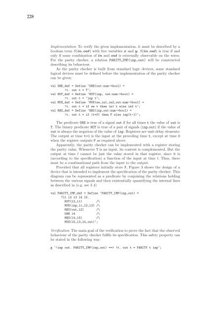
Apparently, the parity checker can be implemented with a register storing<br />
the parity value. Whenever T is an input, its content is complemented. But the<br />
output at time t cannot be just the value stored in that register, since it is<br />
(according to the specification) a function of the input at time t. Thus, there<br />
must be a combinational path from the input to the output.<br />
Provided that all registers initially store F, Figure 3 shows the design of a<br />
device that is intended to implement the specification of the parity checker. This<br />
diagram can be represented as a predicate by conjoining the relations holding<br />
between the various signals and then existentially quantifying the internal lines<br />
as described in (e.g. see 3 4)<br />
val PARITY_IMP_def = Define ‘PARITY_IMP(inp,out) =<br />
?l1 l2 l3 l4 l5.<br />
NOT(l2,l1) /\<br />
MUX(inp,l1,l2,l3) /\<br />
REG(out,l2) /\<br />
ONE l4 /\<br />
REG(l4,l5) /\<br />
MUX(l5,l3,l4,out)‘;<br />
Verification The main goal of the verification to prove the fact that the observed<br />
behaviour of the parity checker fulfils its specification. This safety property can<br />
be stated in the following way:<br />
g ‘!inp out. PARITY_IMP(inp,out) ==> !t. out t = PARITY t inp‘;