- Page 1 and 2:
Author: Patrick J. Kelly Version: 3
- Page 3 and 4:
to get the results described, that
- Page 5 and 6:
The 1982 patent of Heinrich Kunel .
- Page 7 and 8:
Chapter 9: Passive Systems Hans Coh
- Page 9 and 10:
Jesse McQueen . . . . . . . . . . .
- Page 11 and 12:
Spiro Spiros’ COP>1 electrolyser
- Page 13 and 14:
At this point in time - the early y
- Page 15 and 16:
For example, consider a crystal set
- Page 17 and 18:
The actual situation is, that we ar
- Page 19 and 20:
The science taught in schools, coll
- Page 21 and 22:
kinds for sale ready-made. We have
- Page 23 and 24:
Today, we know that these things ar
- Page 25 and 26:
Conventional science says that it c
- Page 27 and 28:
The final shaft drives a standard e
- Page 29 and 30:
efrigerator, for years on end. Conv
- Page 31 and 32:
The electrical pulses to the screen
- Page 33 and 34:
Moray's demonstrations were highly
- Page 35 and 36:
The Colman / Seddon-Gillespie 70-ye
- Page 37 and 38:
Conclusion: The term "Free-Energy"
- Page 39 and 40:
Dan Cook’s self-powered motionles
- Page 41 and 42:
This is the Climachill Ltd. PAC12H
- Page 43 and 44:
A Practical Guide to Free-Energy De
- Page 45 and 46:
There is a patent on the motor but
- Page 47 and 48:
Here, the same shielding idea is ut
- Page 49 and 50:
Or there could be four coils: The c
- Page 51 and 52:
The magnet arrangement is shown her
- Page 53 and 54:
This is a patent which is definitel
- Page 55 and 56:
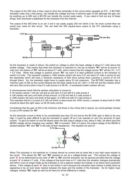
The Jines Permanent Magnet Motor. J
- Page 57 and 58:
Figures 2 and 3 show the position o
- Page 59 and 60:
permanent magnet motor also uses th
- Page 61 and 62:
Shown here is the situation when on
- Page 63 and 64:
It should be remembered that the ti
- Page 65 and 66:
Connecting several coils "in series
- Page 67 and 68:
As this allows the speed to be cont
- Page 69 and 70:
Video presentations on this style o
- Page 71 and 72:
This style of magnet arrangement (N
- Page 73 and 74:
As there is no commentary with the
- Page 75 and 76:
With Dietmar’s design using angle
- Page 77 and 78:
They have not disclosed all of the
- Page 79 and 80:
A square of wood can then be screwe
- Page 81 and 82:
The output shaft spins around one a
- Page 83 and 84:
Fig.2a is an oblique view of the in
- Page 85 and 86:
Fig.6 is a perspective view of the
- Page 87 and 88:
Fig.10 shows the positions of magne
- Page 89 and 90:
Fig.12b shows the arrangement of th
- Page 91 and 92:
The outer stator 3 is composed of t
- Page 93 and 94:
with its end face aligned with the
- Page 95 and 96:
Fig.17a is a schematic representati
- Page 97 and 98:
magnets in all seven series 701 to
- Page 99 and 100:
moves magnets of the opposite polar
- Page 101 and 102:
Each magnet is attracted to the met
- Page 103 and 104:
includes at least one drive magnet
- Page 105 and 106:
Fig.4 is a schematic diagram of one
- Page 107 and 108:
Fig.4 and Fig.5 demonstrate the ori
- Page 109 and 110:
thereby reducing the number transmi
- Page 111 and 112:
In an embodiment of the magnetic dr
- Page 113 and 114:
FIG. 1 is a diagrammatic perspectiv
- Page 115 and 116:
FIG. 5 is a timing diagram showing
- Page 117 and 118:
FIGS. 6A-6H are further timing diag
- Page 119 and 120:
FIG. 10A is a cross-sectional view
- Page 121 and 122:
FIGS. 12A and 12B are enlarged pers
- Page 123 and 124:
1 - 81
- Page 125 and 126:
FIG. 15 is a diagrammatic perspecti
- Page 127 and 128:
FIG. 19 is a perspective view showi
- Page 129 and 130:
material may be used to fabricate t
- Page 131 and 132:
It should be noted that the power z
- Page 133 and 134:
een determined to be quite short, a
- Page 135 and 136:
figure shows the magnet carrier rel
- Page 137 and 138:
Fig.6F shows the magnet carriers 4,
- Page 139 and 140:
Turning now to Figs.8-12B, the magn
- Page 141 and 142:
With continuing reference to Figs.8
- Page 143 and 144:
Although each of the magnetic drive
- Page 145 and 146:
Fig.20 shows another magnetic drive
- Page 147 and 148:
Further, a good deal of experimenta
- Page 149 and 150:
ecause of the tapering of the coppe
- Page 151 and 152:
The diagrams presented by Robert sh
- Page 153 and 154:
Robert Adams has used this construc
- Page 155 and 156:
magnetic materials, each atom has m
- Page 157 and 158:
These outmoded methods have gone on
- Page 159 and 160:
Note on battery tests: I have done
- Page 161 and 162:
2 - 16
- Page 163 and 164:
2 - 18
- Page 165 and 166:
2 - 20
- Page 167 and 168:
2 - 22
- Page 169 and 170:
The unique rotor, briefly described
- Page 171 and 172:
with the mechanical energy that we
- Page 173 and 174:
Those of us interested in the 'free
- Page 175 and 176:
20 0.812 21 0.813 1.5 3.5 21 0.723
- Page 177 and 178:
http://www.totallyamped.net/adams/i
- Page 179 and 180:
The stator preferably comprises a p
- Page 181 and 182:
Fig.4A shows a schematic view of a
- Page 183 and 184:
Fig.7 shows a graphical representat
- Page 185 and 186:
Fig.11 shows a further graphical re
- Page 187 and 188:
A description of the operation of t
- Page 189 and 190:
Although current can be applied to
- Page 191 and 192:
c. When using permanent magnets whi
- Page 193 and 194:
When the permanent magnet is at 0°
- Page 195 and 196:
Therefore if the induced magnetic f
- Page 197 and 198:
coupled to the surface of the rotor
- Page 199 and 200:
Fig.1 depicts a longitudinal cross-
- Page 201 and 202:
Fig.3 depicts a centre cross sectio
- Page 203 and 204:
Fig.5 and Fig.6 depict the interact
- Page 205 and 206:
Fig.7 depicts a longitudinal cross-
- Page 207 and 208:
In Fig.9, the portion of the magnet
- Page 209 and 210:
and recharge a battery bank in the
- Page 211 and 212:
This device is also capable of driv
- Page 213 and 214:
third. This non-linear relationship
- Page 215 and 216:
Fig.4 and Fig.5 illustrate diagramm
- Page 217 and 218:
shaft 103, extend over arcs of appr
- Page 219 and 220:
Fig.3 shows a generator 300 which i
- Page 221 and 222:
In this motor, a series of electrom
- Page 223 and 224:
The housing is divided into three s
- Page 225 and 226:
and having a common point 25. It is
- Page 227 and 228:
Fig.5, a diagrammatic view of a var
- Page 229 and 230:
Fig.1 shows diagrammatically, a mac
- Page 231 and 232:
The gain “g” in power per unit
- Page 233 and 234:
In Fig.7, 110 and 112 designate the
- Page 235 and 236:
The objective is to tune the motor
- Page 237 and 238:
It is suggested that the jumpering
- Page 239 and 240:
T. J. Chorister in America has used
- Page 241 and 242:
You will notice that when the open
- Page 243 and 244:
Doug Konzen has been developing thi
- Page 245 and 246:
The heavy rotor provides some flywh
- Page 247 and 248:
establishment routinely dismiss an
- Page 249 and 250:
Mr Tseung remarks that the large wh
- Page 251 and 252:
Here, just two of the cross timbers
- Page 253 and 254:
With this arrangement, Art states t
- Page 255 and 256:
Here, one pair of brushes is at the
- Page 257 and 258:
The final wire turn goes down throu
- Page 259 and 260:
And as before, the commutator secto
- Page 261 and 262:
Here, the designation “R/S” sta
- Page 263 and 264:
disconnected the motor (the total r
- Page 265 and 266:
A Practical Guide to Free-Energy De
- Page 267 and 268:
common sense but it makes it clear
- Page 269 and 270:
A variation of this arrangement is
- Page 271 and 272:
I wrote an article on this subject,
- Page 273 and 274:
However, all the known transformers
- Page 275 and 276:
Fig.2 shows another embodiment of t
- Page 277 and 278:
Fig.8 shows a stylized dependence o
- Page 279 and 280:
A transformer in accordance with th
- Page 281 and 282:
At a low load resistance (equal to
- Page 283 and 284:
the DC resistance can be minimised
- Page 285 and 286:
Figure 2. C-I and E-I resonant setu
- Page 287 and 288:
available from www.goldwave.com. I
- Page 289 and 290:
other and there are induced magneti
- Page 291 and 292:
The sliding brass contact or “bru
- Page 293 and 294:
understand clearly that the current
- Page 295 and 296:
The blue coil has the power input a
- Page 297 and 298:
efficient working system. The load
- Page 299 and 300:
This is the actual drawing from the
- Page 301 and 302:
(10), which converts the alternatin
- Page 303 and 304:
Figure 4 - shows a third embodiment
- Page 305 and 306:
Fig.2, shows another embodiment of
- Page 307 and 308:
patent application No. BR1020120008
- Page 309 and 310:
facing the north pole of the magnet
- Page 311 and 312:
Fig.2 - is a representation of Fara
- Page 313 and 314:
Fig.7 - is a representation of an e
- Page 315 and 316:
In electron-traps which have numero
- Page 317 and 318:
AWG #4 2.5 turn windings are wound
- Page 319 and 320:
Here are some pictures of Clarence
- Page 321 and 322:
Components used were: Toroids: ----
- Page 323 and 324:
However, the situation changes cons
- Page 325 and 326:
A 110V supply is supposed to swing
- Page 327 and 328:
Lorrie also extended his developmen
- Page 329 and 330:
You will notice that these circuits
- Page 331 and 332:
This original patent application is
- Page 333 and 334:
effect in the primary magnetic path
- Page 335 and 336:
of switch 110 is additive to the ma
- Page 337 and 338:
Fig.7A depicts a preferred construc
- Page 339 and 340:
If this interruption of the flux fl
- Page 341 and 342:
The linear energy generator shown i
- Page 343 and 344:
pulse of the induction flux 5 induc
- Page 345 and 346:
generators which use the transforma
- Page 347 and 348:
This invention relates to a dynamo
- Page 349 and 350:
Fig.3 represents how a flux in the
- Page 351 and 352:
Fig.8 is a fourth embodiment of the
- Page 353 and 354:
The first core 2 and the second cor
- Page 355 and 356:
Next, the power generation efficien
- Page 357 and 358:
magnetic path can be formed in two
- Page 359 and 360:
That is, as indicated in Fig.9, the
- Page 361 and 362:
Stephan states that he has built th
- Page 363 and 364:
This shows clearly that the open en
- Page 365 and 366:
The working pictures of Floyd’s p
- Page 367 and 368:
Frequency generally affected resist
- Page 369 and 370:
Table 1 3 - 105
- Page 371 and 372:
0.72 Mev this which corresponds to
- Page 373 and 374:
The Devices of Don Smith. One free-
- Page 375 and 376:
This circuitry confirms what Don sa
- Page 377 and 378:
The induced electric field exists i
- Page 379 and 380:
When we connect these two plates by
- Page 381 and 382:
direction of rotation to be CCW (Fi
- Page 383 and 384:
This is why we need a high-voltage
- Page 385 and 386:
The above explanation describes the
- Page 387 and 388:
epresent my thoughts and understand
- Page 389 and 390:
The above explanation will help to
- Page 391 and 392:
When the capacitor discharges acros
- Page 393 and 394:
Physically (Fig.23) the electromagn
- Page 395 and 396:
F be the available voltage since th
- Page 397 and 398:
The two yellow capacitors seen abov
- Page 399 and 400:
positions of the magnetic and elect
- Page 401 and 402:
The best combination between the le
- Page 403 and 404:
When converting the reactive electr
- Page 405 and 406:
alternating current. Thousands of T
- Page 407 and 408:
old video, and I recommend everybod
- Page 409 and 410:
general-purpose lighting instead of
- Page 411 and 412:
Video at http://www.youtube.com/wat
- Page 413 and 414:
3 - 149
- Page 415 and 416:
3 - 151
- Page 417 and 418:
An earlier entry on the Chinese for
- Page 419 and 420:
3 - 155
- Page 421 and 422:
In my circuit, the frequency used i
- Page 423 and 424:
Nick has had very impressive result
- Page 425 and 426:
capacitor before being used to driv
- Page 427 and 428:
can be connected together in parall
- Page 429 and 430:
used to do work. The oscillator cir
- Page 431 and 432:
Fig.6 is a section view of a full l
- Page 433 and 434:
Fig.4 is a view of a full-length el
- Page 435 and 436:
inductance, in a receiver, between
- Page 437 and 438:
appear to be not fluctuating at all
- Page 439 and 440:
Accordingly, Fig.2 (which includes
- Page 441 and 442:
and the information then replicated
- Page 443 and 444:
It is actually quite difficult to s
- Page 445 and 446:
The device being displayed is a Tes
- Page 447 and 448:
There is some additional informatio
- Page 449 and 450:
12. Lawrence Tseung has shown how a
- Page 451 and 452:
While this circuit looks like somet
- Page 453 and 454:
A FET has a gate capacitance of abo
- Page 455 and 456:
In the ‘UFOpolitics’ circuit, i
- Page 457 and 458:
My lowest frequency was 133Hz (I ne
- Page 459 and 460:
It is also taught by the prior art,
- Page 461 and 462:
Fig.5 is another alternative arrang
- Page 463 and 464:
Fig.10 is an illustration of an alt
- Page 465 and 466:
Fig.5 shows a coil arrangement 49,
- Page 467 and 468:
The magnetic particle accelerator 1
- Page 469 and 470:
Russ, in his discussion, points out
- Page 471 and 472:
Fig.1 shows the general layout of t
- Page 473 and 474:
Fig.4 above, is an electrical diagr
- Page 475 and 476:
Fig.7 above, illustrates the option
- Page 477 and 478:
The wire end marked “A” will be
- Page 479 and 480:
This shows how completely the (red)
- Page 481 and 482:
Video: http://www.youtube.com/watch
- Page 483 and 484:
If the rotor spins well, then it wo
- Page 485 and 486:
Jacob Byzehr’s Analysis. In 1998,
- Page 487 and 488:
However, the various types of gener
- Page 489 and 490:
The electric drive motor (1) provid
- Page 491 and 492:
Here, the additional output can be
- Page 493 and 494:
The Centrifugal Energy Amplificatio
- Page 495 and 496:
The 25th September 1989 patent appl
- Page 497 and 498:
2. The speed of the wheel turning i
- Page 499 and 500:
https://www.alibaba.com/product-det
- Page 501 and 502:
Presumably, the arm is curved to av
- Page 503 and 504:
The way that the chain manages to p
- Page 505 and 506:
This is because the larger lever ar
- Page 507 and 508:
Admittedly, the deflector pieces wo
- Page 509 and 510:
The question, of course is, will th
- Page 511 and 512:
greater mass of beam A. If an addit
- Page 513 and 514:
likely to be a geared one so that t
- Page 515 and 516:
However, if the linked weights were
- Page 517 and 518:
With this arrangement, the outer we
- Page 519 and 520:
It is pointed out that the lower gu
- Page 521 and 522:
system does not rely on wind, weath
- Page 523 and 524:
Fig.3 shows one version of the firs
- Page 525 and 526:
Fig.9 shows an alternative embodime
- Page 527 and 528:
A Simple Buoyancy Power Generator A
- Page 529 and 530:
Fig.2, is a cross-sectional concept
- Page 531 and 532:
Fig.4, is a perspective conceptual
- Page 533 and 534:
this arrangement is that the tank i
- Page 535 and 536:
again on the ascending side of the
- Page 537 and 538:
The idea is that the liquid on the
- Page 539 and 540:
COP=1200, each household would rece
- Page 541 and 542:
When the system is switched off, th
- Page 543 and 544:
There are, of course, many differen
- Page 545 and 546:
The motor needs to be linked to the
- Page 547 and 548:
For this style of construction, fou
- Page 549 and 550:
Two timber strips 1350 mm long, are
- Page 551 and 552:
It should be explained that, with t
- Page 553 and 554:
This is the position when at rest.
- Page 555 and 556:
A Practical Guide to Free-Energy De
- Page 557 and 558:
current is the same as the earth-ge
- Page 559 and 560:
the local environment, and in this
- Page 561 and 562:
It is recommended that this simple-
- Page 563 and 564:
in the drawing. I strongly recommen
- Page 565 and 566:
and that keeps their operation shor
- Page 567 and 568:
While the above diagram shows each
- Page 569 and 570:
The overall circuit for the opto sw
- Page 571 and 572:
Tests on one of the pure white unit
- Page 573 and 574:
Each base resistor has an output li
- Page 575 and 576:
Or using current day symbols: 5 - 2
- Page 577 and 578:
This current flow through primary w
- Page 579 and 580:
When a bell is struck just once, it
- Page 581 and 582:
pairs from each other, keeping a co
- Page 583 and 584:
No one part of an induction coil ma
- Page 585 and 586:
This insertion of paper increases t
- Page 587 and 588:
This circuit shows the circuit conn
- Page 589 and 590:
desired inductance, and finally, th
- Page 591 and 592:
necessary to get it charged up to 1
- Page 593 and 594:
cyclic connection of the capacitors
- Page 595 and 596:
Fig.2 shows a practical circuit in
- Page 597 and 598:
Fig.6 shows the electrical diagram
- Page 599 and 600:
etween both pairs of batteries. At
- Page 601 and 602:
Fig.6 shows the connection of a dir
- Page 603 and 604:
Walter Ford’s High-powered Crysta
- Page 605 and 606:
oadcast band - say, 1500 kHz - and
- Page 607 and 608:
operating. He runs the circuit driv
- Page 609 and 610:
Quite good lighting can be had from
- Page 611 and 612:
As the LED array lights are essenti
- Page 613 and 614:
The arrangement is for the inner wi
- Page 615 and 616:
With proper modifications this circ
- Page 617 and 618:
When the circuit has been built as
- Page 619 and 620:
With the appropriate modifications
- Page 621 and 622:
We come now to circuits designed by
- Page 623 and 624:
A Suggestion This is an arrangement
- Page 625 and 626:
4. Make sure that the flash is not
- Page 627 and 628:
7. The two switches which form the
- Page 629 and 630:
This “Super Joule Ringer 3.0” c
- Page 631 and 632:
A video of this unit being demonstr
- Page 633 and 634:
Radiant Energy, when converted to e
- Page 635 and 636:
With a pulse duration of 1 microsec
- Page 637 and 638:
Energy stored, multiplied by the cy
- Page 639 and 640:
After careful consideration and man
- Page 641 and 642:
In Joseph Cater’s book “The Awe
- Page 643 and 644:
As it seems to me that there are ma
- Page 645 and 646:
An attempted translation of the pat
- Page 647 and 648:
1. The output voltage does not chan
- Page 649 and 650:
ocaf.org are working with Rosemary'
- Page 651 and 652:
Dr Oleg Gritskevitch’s 1.5 Megawa
- Page 653 and 654:
the dynamo does not accumulate any
- Page 655 and 656:
titanate in the Armenian dynamo was
- Page 657 and 658:
The battery connects at the back, u
- Page 659 and 660:
produce a pulse which keeps the rot
- Page 661 and 662:
Ron Pugh’s Battery Charger. John
- Page 663 and 664:
The magnets embedded in the outer e
- Page 665 and 666:
The three coils have a total of fif
- Page 667 and 668:
6 - 12
- Page 669 and 670:
When a magnet passes the coil conta
- Page 671 and 672:
Although the circuit diagram shows
- Page 673 and 674:
e increased by raising the input vo
- Page 675 and 676:
As you can see, the trick is to pla
- Page 677 and 678:
attery and the charging battery. Fo
- Page 679 and 680:
charging battery and keep doing thi
- Page 681 and 682:
The build used has three electromag
- Page 683 and 684:
not matter either, which way round
- Page 685 and 686:
The Self-Charging Motor. A video at
- Page 687 and 688:
If building a circuit with a solder
- Page 689 and 690:
Alexkor’s Self-Charging Circuit.
- Page 691 and 692:
If the coil is wound on say, a 1.25
- Page 693 and 694:
The coil is tiny, bi-filar wound on
- Page 695 and 696:
If you use the bolt section of one
- Page 697 and 698:
Here, the size of the voltage pulse
- Page 699 and 700:
The simple circuit shown here was u
- Page 701 and 702:
The motor is demonstrated when set
- Page 703 and 704:
This motor is shown running on capa
- Page 705 and 706:
Popp, their evidence is that batter
- Page 707 and 708:
When pin 3 of the 555 goes low, res
- Page 709 and 710:
The 3-Kilowatt Earth Battery This b
- Page 711 and 712:
Magnesium gives excellent results,
- Page 713 and 714:
Einstein, the reality is that it wa
- Page 715 and 716:
Again, it is essential that the wir
- Page 717 and 718:
Please remember that it is Bob Boyc
- Page 719 and 720:
Consequently, it is distinctly poss
- Page 721 and 722:
This is a slightly unusual circuit
- Page 723 and 724:
With an arrangement like that it is
- Page 725 and 726:
It seems probable that this device
- Page 727 and 728:
Fig.1 shows the simplest form, in w
- Page 729 and 730:
It is clear from what has been stat
- Page 731 and 732:
The length of the thin wire coil in
- Page 733 and 734:
Now, consider this circuit as descr
- Page 735 and 736:
have a good aerial connected throug
- Page 737 and 738:
Using two of these boards, Dragan i
- Page 739 and 740:
Thomas developed various versions o
- Page 741 and 742:
The tube of Fig.16 above, uses a di
- Page 743 and 744:
Batteries with their positive and n
- Page 745 and 746:
At last they decided to go up Emigr
- Page 747 and 748:
With the 60 watt lamp and the two c
- Page 749 and 750:
accompanied by corresponding change
- Page 751 and 752:
of these energies. Every part and p
- Page 753 and 754:
When a certain voltage is reached,
- Page 755 and 756:
Herman starts by illustrating how w
- Page 757 and 758:
West direction. However, replicatio
- Page 759 and 760:
In one implementation of the invent
- Page 761 and 762:
Diodes: D1, D2, D3 and D4 - Germani
- Page 763 and 764:
information purposes only” and th
- Page 765 and 766:
This invention converts inertial im
- Page 767 and 768:
SUMMARY OF THE INVENTION The Harmon
- Page 769 and 770:
DETAILED DESCRIPTION OF A PREFERRED
- Page 771 and 772:
What is said in this patent applica
- Page 773 and 774:
But for the Earth's magnetic field,
- Page 775 and 776:
Fig.2 is another diagram further il
- Page 777 and 778:
otor 11 by the charging electrode 1
- Page 779 and 780:
Another object of the present inven
- Page 781 and 782:
Fig.5 is a circuit diagram incorpor
- Page 783 and 784:
Fig.9 is a vertical sectional view
- Page 785 and 786:
extending bars 36 is supported in a
- Page 787 and 788:
In Fig.5, the stator bars are diagr
- Page 789 and 790:
In the system shown in Fig.7, an in
- Page 791 and 792:
In general, the basic electrical sy
- Page 793 and 794:
Initially, at start-up, both of the
- Page 795 and 796:
A Practical Guide to Free-Energy De
- Page 797 and 798:
The people who don’t want self-po
- Page 799 and 800:
First, you have an ordinary air eng
- Page 801 and 802:
This patent shows how the practical
- Page 803 and 804:
Summary of the Invention: These and
- Page 805 and 806:
Fig.3 is a frontal view of the impe
- Page 807 and 808:
Fig.7 is a perspective view of a se
- Page 809 and 810:
The front housing section 32 is a h
- Page 811 and 812:
transition duct 96 is believed to r
- Page 813 and 814:
slightly curved. The blades gradual
- Page 815 and 816:
With respect to the application of
- Page 817 and 818:
This results in the air temperature
- Page 819 and 820:
The operating pressure produced by
- Page 821 and 822:
Josef never managed to get his engi
- Page 823 and 824:
petroleum products to operate. Mich
- Page 825 and 826:
This invention relates generally to
- Page 827 and 828:
working fluid opening which may be
- Page 829 and 830:
7. The heat pump of claim 6 wherein
- Page 831 and 832:
Fig.3 is a cross section and Fig.4
- Page 833 and 834:
In Fig.3, a rotor for a unit using
- Page 835 and 836:
US Patent 3,931,713 13th January 19
- Page 837 and 838:
Fig.3 is a cross section of another
- Page 839 and 840:
Fig.2 shows an end view of the unit
- Page 841 and 842:
The vanes of the rotors may be made
- Page 843 and 844:
thinking of it as a fuel-less or se
- Page 845 and 846:
Proprietary liquids, specifically c
- Page 847 and 848:
Additional warm air to augment air
- Page 849 and 850:
And the schematic diagram is: One e
- Page 851 and 852:
Thomas is by no means the first per
- Page 853 and 854:
more than a minute or so. If there
- Page 855 and 856:
According to this invention, the bl
- Page 857 and 858:
The frame of the pyramid is not the
- Page 859 and 860:
The very fine filter-grade quartz s
- Page 861 and 862:
The capacitor is positioned inside
- Page 863 and 864:
Thomas’ website which is in Germa
- Page 865 and 866:
frame pyramids. This area is wide o
- Page 867 and 868:
James invites you to run this test
- Page 869 and 870:
(2) Placing an insulated coil on th
- Page 871 and 872:
ut in time you will see the tremend
- Page 873 and 874:
used within its glass walls. Pest-f
- Page 875 and 876:
to eat it, but if I was going to pr
- Page 877 and 878:
had the same sensations of coldness
- Page 879 and 880:
which are much closer to those of t
- Page 881 and 882:
Photographs 1 and 2 show two differ
- Page 883 and 884:
destructive phenomena, you destroy
- Page 885 and 886:
The Cell itself is made up with the
- Page 887 and 888:
Seven or eight stainless steel cone
- Page 889 and 890:
part of the diagram. Cut another wa
- Page 891 and 892:
This arrangement looks more complic
- Page 893 and 894:
aligned. The spacers will be more e
- Page 895 and 896:
mode was being used. The surprising
- Page 897 and 898:
operates by breaking water down int
- Page 899 and 900:
In the installation shown above, yo
- Page 901 and 902:
If tack-welded cylinders have to be
- Page 903 and 904:
As stated earlier, the first 5 mile
- Page 905 and 906:
airtight! Go and do something else.
- Page 907 and 908:
engine starts to ping. When the tim
- Page 909 and 910:
It should be clearly understood tha
- Page 911 and 912:
Comments from an expert in July 201
- Page 913 and 914:
To be sure that the second and thir
- Page 915 and 916:
The claims made for this coil are q
- Page 917 and 918:
encouraging you personally to try t
- Page 919 and 920:
idea of the universe which you have
- Page 921 and 922:
A: There are several workshops wher
- Page 923 and 924:
A Practical Guide to Free-Energy De
- Page 925 and 926:
the Space Shuttle into space! If yo
- Page 927 and 928:
circuit and each power socket circu
- Page 929 and 930:
The plate shapes shown above are ar
- Page 931 and 932:
Any of these designs can be 6-cell
- Page 933 and 934:
and so has to be accepted as an ove
- Page 935 and 936:
A good source for general component
- Page 937 and 938:
To deal with this, a one-way valve
- Page 939 and 940:
A point which might not be immediat
- Page 941 and 942:
The method which Zach uses is somew
- Page 943 and 944:
It is always difficult to make a go
- Page 945 and 946:
If, in spite of all precautions, yo
- Page 947 and 948:
shock-wave when it is ignited so th
- Page 949 and 950:
Caution: This electrolyser is not a
- Page 951 and 952:
The items marked with a blue dot fo
- Page 953 and 954:
The six electrolyser cells and the
- Page 955 and 956:
When used with rainwater from a bar
- Page 957 and 958:
The arrangement with three cells co
- Page 959 and 960:
It is available from ship’s chand
- Page 961 and 962:
This second layer is wound in exact
- Page 963 and 964:
who is outstanding in this field is
- Page 965 and 966:
The technique of DC pulsing require
- Page 967 and 968:
The bolts tapped into the inner tub
- Page 969 and 970:
These arms get two bends in them in
- Page 971 and 972:
In this rather unusual circuit, the
- Page 973 and 974:
Circuit operation: The main part of
- Page 975 and 976:
second. The larger the capacitor, t
- Page 977 and 978:
Here, the 555 chip output voltage i
- Page 979 and 980:
The underside of the strip-board (w
- Page 981 and 982:
Component Quantity Description Comm
- Page 983 and 984:
conventional electricity, and it ha
- Page 985 and 986:
The outer pipes are drilled and tap
- Page 987 and 988:
method is by powering the cell up f
- Page 989 and 990:
Dr. Cramton says: “I would like p
- Page 991 and 992:
Dave Lawton’s Auto-Tune Circuit.
- Page 993 and 994:
Because of these things, the calcul
- Page 995 and 996:
Here, they have opted to feed the H
- Page 997 and 998:
Diesel has the same structure but w
- Page 999 and 1000:
we definitely do not want that to h
- Page 1001 and 1002:
Making the HHO gas When the generat
- Page 1003 and 1004:
Boyce would need 400 watts without
- Page 1005 and 1006:
• Powder Coated Finish • Light
- Page 1007 and 1008:
The ball is held in place by the sp
- Page 1009 and 1010:
The pipes, backing plate, pressure-
- Page 1011 and 1012:
for a year. The objective is to del
- Page 1013 and 1014:
5. Next comes a bit of arithmetic.
- Page 1015 and 1016:
The copper pipe is then heated with
- Page 1017 and 1018:
The water is then treated by insert
- Page 1019 and 1020:
greater pressure on the piston duri
- Page 1021 and 1022:
The first part of David Quirey’s
- Page 1023 and 1024:
Let me stress that this is just an
- Page 1025 and 1026:
and while, not surprisingly, I have
- Page 1027 and 1028:
Developed in conjunction with the E
- Page 1029 and 1030:
electrical generator. The engine ra
- Page 1031 and 1032:
The sole explanation of the explosi
- Page 1033 and 1034:
This turbine creates a spinning air
- Page 1035 and 1036:
Ted created the egg-shaped part of
- Page 1037 and 1038:
degrees. With it’s 350 cubic inch
- Page 1039 and 1040:
Roger Maynard’s Water Vapour Inje
- Page 1041 and 1042:
“Fuelsavers” Streamlining Fins.
- Page 1043 and 1044:
I started out in 1976 when the firs
- Page 1045 and 1046:
properly, saving the government a l
- Page 1047 and 1048:
educed accordingly. If the Gen III
- Page 1049 and 1050:
flow. This is a useful energy gain
- Page 1051 and 1052:
This is an unusual voltage-doubler
- Page 1053 and 1054:
While on the other hand, if negativ
- Page 1055 and 1056:
describes many possible application
- Page 1057 and 1058:
Suartt and Gourley realised that th
- Page 1059 and 1060:
produced by this process is likely
- Page 1061 and 1062:
Fig.4 illustrates graphs showing th
- Page 1063 and 1064:
which do not provoke electrolysis o
- Page 1065 and 1066:
SG Gas, the tank was decompressed a
- Page 1067 and 1068:
Fig.5 shows a typical absorption ov
- Page 1069 and 1070:
Biological Properties Transport, De
- Page 1071 and 1072:
This reaction changes water from a
- Page 1073 and 1074:
With this unit, air is sucked out o
- Page 1075 and 1076:
etween these plates, these craters
- Page 1077 and 1078:
In the years leading up to 1970, ex
- Page 1079 and 1080:
These sanctions which were initiate
- Page 1081 and 1082:
spotlight, and yet, he is carrying
- Page 1083 and 1084:
A Practical Guide to Free-Energy De
- Page 1085 and 1086:
does not appear to be any reason wh
- Page 1087 and 1088:
Brief Description of the Drawings F
- Page 1089 and 1090:
aether phase-lock cannot force the
- Page 1091 and 1092:
Referring to Fig.2, the inductors 3
- Page 1093 and 1094:
combination of the two capacitor-in
- Page 1095 and 1096:
power by tapping energy from space.
- Page 1097 and 1098:
to the innermost electrodes. This m
- Page 1099 and 1100:
state” exhibiting the attributes
- Page 1101 and 1102:
The force of the Zero-Point Energy
- Page 1103 and 1104:
If you find the concept of producin
- Page 1105 and 1106:
ook, also later in this chapter, po
- Page 1107 and 1108:
(B) (i) The orthodox view of a heli
- Page 1109 and 1110:
Electromagnetic output is a functio
- Page 1111 and 1112:
When you place a magnet on the door
- Page 1113 and 1114:
11 - 31
- Page 1115 and 1116:
The outer magnets in the diagram ab
- Page 1117 and 1118:
He also suggests that monopole grav
- Page 1119 and 1120:
Here, there is no net electrical or
- Page 1121 and 1122:
Ferrite is a better material for th
- Page 1123 and 1124:
Joseph has been granted a patent an
- Page 1125 and 1126:
The next interesting point is that
- Page 1127 and 1128:
Joseph then went on to consider the
- Page 1129 and 1130:
Maxwell says that there is a vast s
- Page 1131 and 1132:
In any given instant of time, the a
- Page 1133 and 1134:
magnet of some 600 pounds in weight
- Page 1135 and 1136:
Davis makes the following observati
- Page 1137 and 1138:
coil should be wound in the same di
- Page 1139 and 1140:
Edmund says: Each output coils’ h
- Page 1141 and 1142:
use of any heating fuel. This next
- Page 1143 and 1144:
1009908 November 1911 Lafore 111594
- Page 1145 and 1146:
pressure of the gas being entrained
- Page 1147 and 1148:
turbines and pumps and so are not d
- Page 1149 and 1150:
Fig.1 shows a heat transfer system
- Page 1151 and 1152:
DETAILED DESCRIPTION Referring to F
- Page 1153 and 1154:
When operating, a voltage is applie
- Page 1155 and 1156:
US 3,065,935, Duberry/Frost/Earl US
- Page 1157 and 1158:
This small selection of forty-six p
- Page 1159 and 1160:
In addition, Nieper established the
- Page 1161 and 1162:
Means of Operation The device is st
- Page 1163 and 1164:
In late 2001, I wrote a magazine ar
- Page 1165 and 1166:
of matter and is nothing more than
- Page 1167 and 1168:
Hypothetically, is certainly the in
- Page 1169 and 1170:
7. Nieper, Hans A., Ph.D., 1985, Co
- Page 1171 and 1172:
Summary: In accordance with the pre
- Page 1173 and 1174:
Fig.5A and Fig.5B are schematic par
- Page 1175 and 1176:
Referring now to Figs 2, 3 and 4 in
- Page 1177 and 1178:
According to the embodiment of the
- Page 1179 and 1180:
invention does not perform any subs
- Page 1181 and 1182:
I’m a geologist. And the one thin
- Page 1183 and 1184:
one of them took the bacteria, deve
- Page 1185 and 1186:
Bob Beck’s Electronic Pulser. The
- Page 1187 and 1188:
There is a parts list on page 4 tha
- Page 1189 and 1190:
This is a theory: about 30% of the
- Page 1191 and 1192:
Finance: Money only has value when
- Page 1193 and 1194:
Moon, a seismic detector left on th
- Page 1195 and 1196:
of a particle is inversely proporti
- Page 1197 and 1198:
It now becomes evident, why a mass
- Page 1199 and 1200:
intensity of these zones, determine
- Page 1201 and 1202:
The leading part of the gravity rad
- Page 1203 and 1204:
light has to be of high intensity.
- Page 1205 and 1206:
freezing point, the molecular activ
- Page 1207 and 1208:
apparently a factor in it’s perfo
- Page 1209 and 1210:
the surface area is sufficient to a
- Page 1211 and 1212:
least squares. Conventional statist
- Page 1213 and 1214:
the insulation and stop at the surf
- Page 1215 and 1216:
together and the resulting ethers e
- Page 1217 and 1218:
any other type of radiation such as
- Page 1219 and 1220:
an orgone accumulator. ------------
- Page 1221 and 1222:
There are several different types o
- Page 1223 and 1224:
Examples: Red, Red, Red: 2 2 00 ohm
- Page 1225 and 1226: As before, the colour coding is exa
- Page 1227 and 1228: This determination of the voltage l
- Page 1229 and 1230: If a bulb is used instead of R2, th
- Page 1231 and 1232: at about 8 Volts. We can use Ohm’
- Page 1233 and 1234: Then the LED gets connected to the
- Page 1235 and 1236: transistor. A gain of 200 means tha
- Page 1237 and 1238: Here, an additional transistor (‘
- Page 1239 and 1240: The design covered above is not the
- Page 1241 and 1242: With this circuit, two ordinary dio
- Page 1243 and 1244: This is not an FET transistor and s
- Page 1245 and 1246: functioning. If the Power Supply Un
- Page 1247 and 1248: devices, immune to shock and vibrat
- Page 1249 and 1250: The main difference being that when
- Page 1251 and 1252: The strength of the magnetic field
- Page 1253 and 1254: Instead, if you connect the 10 Volt
- Page 1255 and 1256: This produces a much better result
- Page 1257 and 1258: Multivibrators: The Bistable. The n
- Page 1259 and 1260: 2. The press-button switch is opera
- Page 1261 and 1262: Here, The input impedance has been
- Page 1263 and 1264: Here, a slow-running astable is sub
- Page 1265 and 1266: time. Small fingers and good eyesig
- Page 1267 and 1268: shown on the right. There is now a
- Page 1269 and 1270: in this voltage level since it is b
- Page 1271 and 1272: Astable Frequencies 100 470 1K 4.7K
- Page 1273 and 1274: http://www.talkingelectronics.com/p
- Page 1275: ohm resistor in the output line whi
- Page 1279 and 1280: Bob Beck’s design calls for the L
- Page 1281 and 1282: The two 18V zener diodes drop off 1
- Page 1283 and 1284: To avoid shock liability, use batte
- Page 1285 and 1286: Here, the gain is set by the ratio
- Page 1287 and 1288: This circuit is set up as evening f
- Page 1289 and 1290: There are three connections to the
- Page 1291 and 1292: If pin 14 is provided with the outp
- Page 1293 and 1294: In this example, the sequence is st
- Page 1295 and 1296: single chip, and which is called a
- Page 1297 and 1298: The last line "goto Main" tells the
- Page 1299 and 1300: Capacitors. We have avoided mention
- Page 1301 and 1302: The time has come for a serious war
- Page 1303 and 1304: DC we would multiply them together
- Page 1305 and 1306: These have a coil of wire wound aro
- Page 1307 and 1308: For the moment, we will ignore the
- Page 1309 and 1310: Relay switching is not so critical
- Page 1311 and 1312: The first strand of the coil starts
- Page 1313 and 1314: The decoupling is to provide the 55
- Page 1315 and 1316: It can also be useful to have a ver
- Page 1317 and 1318: So, when you are deciding what mult
- Page 1319 and 1320: Resistor ‘VR1’ is padded with t
- Page 1321 and 1322: output meter display to zero when t
- Page 1323 and 1324: attery to an electrical circuit, th
- Page 1325 and 1326: The major physical principles invol
- Page 1327 and 1328:
Another possibility is that the jar
- Page 1329 and 1330:
However, when this is done, the bru
- Page 1331 and 1332:
The circuit shown here is broken by
- Page 1333 and 1334:
and build a release field. Then the
- Page 1335 and 1336:
No hydrogen is consumed. No additio
- Page 1337 and 1338:
alone more than 100%. This system w
- Page 1339 and 1340:
completely to show that there was n
- Page 1341 and 1342:
Numbers used on the schematic: 1- A
- Page 1343 and 1344:
BACKGROUND OF THE INVENTION Electri
- Page 1345 and 1346:
power the electric motor. The secon
- Page 1347 and 1348:
un using air and hydrogen as the fu
- Page 1349 and 1350:
nuts tightened on a 10 mm (3/8”)
- Page 1351 and 1352:
The inner nuts are manoeuvred on in
- Page 1353 and 1354:
just the relay current to be handle
- Page 1355 and 1356:
The bolt is kept just clear of the
- Page 1357 and 1358:
4. How do you determine the amount
- Page 1359 and 1360:
Electrical Generation: The cell wil
- Page 1361 and 1362:
From another user: Hi, thanks for t
- Page 1363 and 1364:
These two cells have been in use in
- Page 1365 and 1366:
urning status should you choose to
- Page 1367 and 1368:
There are also many problems with t
- Page 1369 and 1370:
This looks as if the pressure tank
- Page 1371 and 1372:
The objective is to get two stainle
- Page 1373 and 1374:
If a standard laminated iron yoke i
- Page 1375 and 1376:
paranoid reaction. Perhaps, I would
- Page 1377 and 1378:
Closed Systems and Open Systems If
- Page 1379 and 1380:
an open system, which brings us to
- Page 1381 and 1382:
captures all of the magnetic field
- Page 1383 and 1384:
Because the MEG is an open system,
- Page 1385 and 1386:
Note that the M1 coil is reversed.
- Page 1387 and 1388:
A Practical Guide to Free-Energy De
- Page 1389 and 1390:
Wood of any type, branches, sticks,
- Page 1391 and 1392:
http://www.woodgas.net/index.html -
- Page 1393 and 1394:
A system like this needs extreme ca
- Page 1395 and 1396:
Mr Kim also shows a burner intended
- Page 1397 and 1398:
Sterling’s web site is definitely
- Page 1399 and 1400:
The “heat exchanger” is a radia
- Page 1401 and 1402:
Peter Davey’s AC Heater. During W
- Page 1403 and 1404:
http://www.overunity.com/index.php?
- Page 1405 and 1406:
14 - 19
- Page 1407 and 1408:
I changed the connections inside my
- Page 1409 and 1410:
This view shows two important featu
- Page 1411 and 1412:
a good angle when flowing through t
- Page 1413 and 1414:
existing methods. The parabolic coo
- Page 1415 and 1416:
Construction Steps Cut a Half-circl
- Page 1417 and 1418:
The easiest way to do this is to pu
- Page 1419 and 1420:
usual, to trap the heat. The suspen
- Page 1421 and 1422:
Cooking times are approximate. Incr
- Page 1423 and 1424:
spread this technology is to encour
- Page 1425 and 1426:
on opposite ends of the funnel is f
- Page 1427 and 1428:
The power is found in Watts. A powe
- Page 1429 and 1430:
cookers provide a sustainable techn
- Page 1431 and 1432:
How can one readily determine if th
- Page 1433 and 1434:
IDEXX Laboratories, Inc. makes the
- Page 1435 and 1436:
pulled back to let the condensation
- Page 1437 and 1438:
Mark the underside of the flaps of
- Page 1439 and 1440:
This effect is very noticeable on f
- Page 1441 and 1442:
By applying these same methods on a
- Page 1443 and 1444:
14 - 57
- Page 1445 and 1446:
It is, of course, essential for the
- Page 1447 and 1448:
ATMOSPHERIC WATER SUPPLY APPARATUS
- Page 1449 and 1450:
Fig.3 is a sectional view taken sub
- Page 1451 and 1452:
Referring now to figures 2, 3, 4 an
- Page 1453 and 1454:
Another system is using a large Fre
- Page 1455 and 1456:
5. Antibiotics have no impact whats
- Page 1457 and 1458:
For a decade, Musk’s startup call
- Page 1459 and 1460:
Arthur Bentley’s Water Pump. The
- Page 1461 and 1462:
The performance of a Ram Pump is im
- Page 1463 and 1464:
small flies, by hanging polythene b
- Page 1465 and 1466:
This has the very considerable adva
- Page 1467 and 1468:
Also, a two-part article on Solar c
- Page 1469 and 1470:
terminates in a distributor head 31
- Page 1471 and 1472:
do your own checking as designs cha
- Page 1473 and 1474:
Rated at up to 3 Amp-Hour capacity,
- Page 1475 and 1476:
The only moving component in this s
- Page 1477 and 1478:
------------------- Without knowing
- Page 1479 and 1480:
Here, the extra switch marked “BO
- Page 1481 and 1482:
If there are not wires already atta
- Page 1483 and 1484:
10. It is much easier to work on th
- Page 1485 and 1486:
14. The final connections which nee
- Page 1487 and 1488:
17. Connect a voltmeter across the
- Page 1489 and 1490:
The same voltage reading should be
- Page 1491 and 1492:
This is making a connection between
- Page 1493 and 1494:
---------------------- There are ot
- Page 1495 and 1496:
While these particular units have j
- Page 1497 and 1498:
With fully charged batteries switch
- Page 1499 and 1500:
360 Degree Lighting for Africa The
- Page 1501 and 1502:
If ordinary 10-battery holders are
- Page 1503 and 1504:
echarging mobile phones. It should
- Page 1505 and 1506:
These metres show more than 100-wat
- Page 1507 and 1508:
The pads are kept wet by droplets o
- Page 1509 and 1510:
This one at https://www.youtube.com
- Page 1511 and 1512:
The objective is to make a home whi
- Page 1513 and 1514:
The overall design is set up for co
- Page 1515 and 1516:
The constructional details can be f
- Page 1517 and 1518:
When the wall is finished off and t
- Page 1519 and 1520:
The important thing to remember abo
- Page 1521 and 1522:
There was one group of landowners w
- Page 1523 and 1524:
If you feel that these things are a
- Page 1525 and 1526:
you at all unless you consent to be
- Page 1527 and 1528:
Do you feel that you are obliged to
- Page 1529 and 1530:
purchased was transported to the sh
- Page 1531 and 1532:
the enemy of the United States Gove
- Page 1533 and 1534:
loans at interest, and that was the
- Page 1535 and 1536:
of the Federal Reserve, there was n
- Page 1537 and 1538:
world trade system and to build up
- Page 1539 and 1540:
have enough gold to cover the outst
- Page 1541 and 1542:
But understand this above all else,
- Page 1543 and 1544:
Iran 1953: The precedent for econom
- Page 1545 and 1546:
Panama 1981: Omar Tarrijas Presiden
- Page 1547 and 1548:
doesn’t. And in the case of Iraq,
- Page 1549 and 1550:
Inspector of Schools, has recently
- Page 1551 and 1552:
every useful forum with a combinati
- Page 1553 and 1554:
anything about keeping to a speed l
- Page 1555 and 1556:
delivered to them. The financial in
- Page 1557 and 1558:
above mentioned papers and readily
- Page 1559 and 1560:
Patent. Under no circumstances hear
- Page 1561 and 1562:
and appurtenances… we perform and
- Page 1563 and 1564:
went - to the Crown Temple. This sh
- Page 1565 and 1566:
WMAQ - Chicago WCAU - Philadelphia
- Page 1567 and 1568:
Sweden and wife of King Gustav. Lou
- Page 1569 and 1570:
Silent weapon technology has evolve
- Page 1571 and 1572:
sources of natural and social energ
- Page 1573 and 1574:
association of consumer preferences
- Page 1575 and 1576:
(a few examples will be given.) Cha
- Page 1577 and 1578:
Economic Shock Testing In recent ti
- Page 1579 and 1580:
Liabilities: (1) Creditors (2) Enem
- Page 1581 and 1582:
(10) Controls manufacturing. (11) C
- Page 1583 and 1584:
If this rise of the lower classes c
- Page 1585 and 1586:
oken down into categories by intell
- Page 1587 and 1588:
Further, there are no penalties in
- Page 1589 and 1590:
And showing the flattening of the g
- Page 1591 and 1592:
Here, the poorest billion people wa
- Page 1593 and 1594:
This states that it is a crime to p
- Page 1595 and 1596:
A Practical Guide to Free-Energy De
- Page 1597 and 1598:
It is not necessary to "go for brok
- Page 1599 and 1600:
Another device which is not hard to
- Page 1601 and 1602:
as that, but perhaps one of say, th
- Page 1603 and 1604:
Devices Which are the Easiest to Bu
- Page 1605 and 1606:
whether or not there are any genera
- Page 1607 and 1608:
Ron Classen has replicated this des
- Page 1609 and 1610:
devices have to be rated as some of
- Page 1611 and 1612:
This design appeals to most people
- Page 1613 and 1614:
Thomas Henry Moray’s Aerial Syste
- Page 1615 and 1616:
Do you have any values for Peter Lo
- Page 1617 and 1618:
so I suggest that you begin with an
- Page 1619 and 1620:
electrolyzer following your plans a
- Page 1621 and 1622:
which he used to power an electrica
- Page 1623 and 1624:
You state in the literature that th
- Page 1625 and 1626:
"How 2 Fix To create a power source
- Page 1627 and 1628:
My frequency reads 35.4 KHz or 3540
- Page 1629 and 1630:
wire length ratio between L1 and L2
- Page 1631 and 1632:
So, if you let your high-frequency
- Page 1633 and 1634:
Question: I may have missed any dis
- Page 1635 and 1636:
Question: Always been a fan of your
- Page 1637 and 1638:
You will notice that each of these
- Page 1639 and 1640:
This circuit will have all three tr
- Page 1641 and 1642:
Chapter 17: An Easy-Build Generator
- Page 1643 and 1644:
Each plank is supplied with a facto
- Page 1645 and 1646:
It is suggested that the rotor is d
- Page 1647 and 1648:
A really major advantage of this ty
- Page 1649 and 1650:
This arrangement has sixteen coils,
- Page 1651 and 1652:
drill blocks the view from vertical
- Page 1653 and 1654:
We now want to cut out the rotor (b
- Page 1655 and 1656:
Leave 30 mm below the lowest plank
- Page 1657 and 1658:
These saw sets normally have a saw
- Page 1659 and 1660:
eaches that of the second highest v
- Page 1661 and 1662:
This arrangement allows complete fl
- Page 1663 and 1664:
This transistor is popular and is a
- Page 1665 and 1666:
You will notice that there is a dio
- Page 1667 and 1668:
If you prefer not to make coil spoo
- Page 1669 and 1670:
A Practical Guide to Free-Energy De
- Page 1671 and 1672:
Fig. 4. Explanation of the principl
- Page 1673 and 1674:
Fig. 7. The simplest manifestation
- Page 1675 and 1676:
Fig. 10. Using asymmetrical electro
- Page 1677 and 1678:
Fig.14 Voltage distribution on the
- Page 1679 and 1680:
Fig. 18 Schematic from the Donald S
- Page 1681 and 1682:
Chapter 19: Building A Motor / Gene
- Page 1683 and 1684:
John’s design starts with a DC mo
- Page 1685 and 1686:
John says that he tunes his design
- Page 1687 and 1688:
If you are careful to get the centr
- Page 1689 and 1690:
Cut out the marked lines and work t
- Page 1691 and 1692:
to the battery to recharge it. Inst
- Page 1693 and 1694:
A Practical Guide to Free-Energy De
- Page 1695 and 1696:
The performance is most impressive
- Page 1697 and 1698:
Driven by an AC mains motor, once r
- Page 1699 and 1700:
With this “stick welder” the si
- Page 1701 and 1702:
For this construction, each of the
- Page 1703 and 1704:
We need to pass a mild steel pipe t
- Page 1705 and 1706:
The spokes are made with 50 mm x 50
- Page 1707 and 1708:
There are a few additions to be mad
- Page 1709 and 1710:
All right, that is the first way to
- Page 1711 and 1712:
No matter what tool is used, don’
- Page 1713 and 1714:
It is not at all easy to take a wel
- Page 1715 and 1716:
This diagram shows only one drive m
- Page 1717 and 1718:
In the position shown, the Generato
- Page 1719 and 1720:
ase of the transistor, causing it t
- Page 1721 and 1722:
of plastic pipe which prevents the
- Page 1723 and 1724:
where the direction of twist revers
- Page 1725 and 1726:
This arrangement allows the value o
- Page 1727 and 1728:
The load could be buffered from the
- Page 1729 and 1730:
The idea here is that the reels of
- Page 1731 and 1732:
An American contributor who prefers
- Page 1733 and 1734:
commercially and which is covered i
- Page 1735 and 1736:
shelf and a narrow shelf. The sides
- Page 1737 and 1738:
22-8
- Page 1739 and 1740:
If you intend to paint the housing,
- Page 1741 and 1742:
The ‘Variac’ variable mains tra
- Page 1743 and 1744:
This has the effect of overcoming a
- Page 1745 and 1746:
The NST unit is readily available a
- Page 1747 and 1748:
We now come to the items which we n
- Page 1749 and 1750:
However, the overall arrangement sh
- Page 1751 and 1752:
This board is called type “B” a
- Page 1753 and 1754:
One detail to be mentioned is the t
- Page 1755 and 1756:
The idea is to cut a groove or chan
- Page 1757 and 1758:
to the two ends of my first number
- Page 1759 and 1760:
the setting up of your machine. Fai
- Page 1761 and 1762:
Socket Surge Protector Strip Plug E
- Page 1763 and 1764:
Appendix TABLE OF WIRE SIZES: The w
- Page 1765 and 1766:
Briefly stated, the present inventi
- Page 1767 and 1768:
shaped magnet having a rear side an
- Page 1769 and 1770:
Fig.2 is a schematic plan view of a
- Page 1771 and 1772:
Fig.7A is a schematic plan view of
- Page 1773 and 1774:
Fig.9 is a schematic perspective vi
- Page 1775 and 1776:
Fig.12 is an end elevational view o
- Page 1777 and 1778:
Fig.15B is an end elevational view
- Page 1779 and 1780:
Fig.19 is an elevational end view o
- Page 1781 and 1782:
further aspect of the rotor 12, as
- Page 1783 and 1784:
the U-shaped magnets 20 having subs
- Page 1785 and 1786:
Referring now to Fig.1B, Fig.2 and
- Page 1787 and 1788:
an axis 16 of the rotor 12. The mot
- Page 1789 and 1790:
Preferably, the surface 64 of the s
- Page 1791 and 1792:
A - 29
- Page 1793 and 1794:
Referring now to Fig.6, Fig.7D and
- Page 1795 and 1796:
each first stator magnet 40, is loc
- Page 1797 and 1798:
Referring now to Fig.2, Fig.3, Fig.
- Page 1799 and 1800:
12 and three pairs 32 of U-shaped m
- Page 1801 and 1802:
about an armature axis of rotation
- Page 1803 and 1804:
Referring now to Fig.5, Fig.16 and
- Page 1805 and 1806:
otor 12. Further the number of abut
- Page 1807 and 1808:
11. The apparatus (10') of claim 7,
- Page 1809 and 1810:
causes the unpaired electrons to sp
- Page 1811 and 1812:
A - 49
- Page 1813 and 1814:
Fig.4, and the spinning electron pa
- Page 1815 and 1816:
the armature magnets for given magn
- Page 1817 and 1818:
23. The method of producing a unidi
- Page 1819 and 1820:
use of a rotating carousel which ca
- Page 1821 and 1822:
Fig.4 is a cross-sectional view of
- Page 1823 and 1824:
Fig.7 is a wave form showing flux l
- Page 1825 and 1826:
Fig.14 is a modification of the car
- Page 1827 and 1828:
surface of channel 28. This arrange
- Page 1829 and 1830:
the magnetic field. An examination
- Page 1831 and 1832:
induced in coil 17 is a function of
- Page 1833 and 1834:
The modified carousel structure 24'
- Page 1835 and 1836:
Notes: I found it a little difficul
- Page 1837 and 1838:
Fig.2 is a schematic layout of a hi
- Page 1839 and 1840:
Extending from switches 14 and 16 i
- Page 1841 and 1842:
Table 1 shows the data to be obtain
- Page 1843 and 1844:
Across a single fluorescent lamp, t
- Page 1845 and 1846:
HAROLD COLMAN & RONALD SEDDON-GILLE
- Page 1847 and 1848:
The ends of the quartz tube 13 are
- Page 1849 and 1850:
JONG-SOK AN: NO-LOAD GENERATOR Pate
- Page 1851 and 1852:
In short, the present invention is
- Page 1853 and 1854:
Fig.4 is an enlarged plan view of m
- Page 1855 and 1856:
BEST MODES FOR CARRYING OUT THE INV
- Page 1857 and 1858:
As shown in Fig.3, the coils are wo
- Page 1859 and 1860:
When electric power is to be genera
- Page 1861 and 1862:
As shown in Table 3 above, as the r
- Page 1863 and 1864:
SUMMARY OF THE INVENTION The Contin
- Page 1865 and 1866:
Fig.2 shows an internal wiring diag
- Page 1867 and 1868:
Fig.5 shows a wiring diagram for an
- Page 1869 and 1870:
Fig.8 shows the complete system of
- Page 1871 and 1872:
Fig.2 shows the three-phase arrange
- Page 1873 and 1874:
Once the generator is started, a sm
- Page 1875 and 1876:
MICHAEL OGNYANOV: SEMICONDUCTORS Pa
- Page 1877 and 1878:
Fig.3 is an electric circuit diagra
- Page 1879 and 1880:
The lead 39 is also connected to on
- Page 1881 and 1882:
EDWIN GRAY: ELECTRIC MOTOR US Paten
- Page 1883 and 1884:
Fig.1 is an explanatory schematic d
- Page 1885 and 1886:
Fig.5 is a sectional view taken at
- Page 1887 and 1888:
Fig.11 is a sectional view taken at
- Page 1889 and 1890:
Fig.14 is a sectional view, taken a
- Page 1891 and 1892:
Fig.19 is a developed view, taken a
- Page 1893 and 1894:
Referring to Fig.4, Fig.5 and Fig.9
- Page 1895 and 1896:
At a position 13.33 degrees to the
- Page 1897 and 1898:
start of a cycle are shown to corre
- Page 1899 and 1900:
Clutch 304 is associated with shaft
- Page 1901 and 1902:
in rotation by the successive disch
- Page 1903 and 1904:
Means for discharging said charged
- Page 1905 and 1906:
DESCRIPTION OF THE PREFERRED EMBODI
- Page 1907 and 1908:
inductance 36, inducing a strong el
- Page 1909 and 1910:
solid-state commutator, that closes
- Page 1911 and 1912:
2.7K cosmic background temperature
- Page 1913 and 1914:
disc. Also, the rotor may be mounte
- Page 1915 and 1916:
Fig.3 depicts the magnetisation act
- Page 1917 and 1918:
The fact that one can extract energ
- Page 1919 and 1920:
In the situation depicted in Fig.2
- Page 1921 and 1922:
the flux will be attracted through
- Page 1923 and 1924:
In the latter case it would still s
- Page 1925 and 1926:
otor, rotor magnetisation means inc
- Page 1927 and 1928:
unit of radium to the wire was elim
- Page 1929 and 1930:
The output coil is positioned so as
- Page 1931 and 1932:
Fig.2A is a perspective view schema
- Page 1933 and 1934:
Fig.6 is a perspective view of the
- Page 1935 and 1936:
Fig.9B is a schematic end-view of t
- Page 1937 and 1938:
The only physicist to recognise in
- Page 1939 and 1940:
like recoil of an electron when it
- Page 1941 and 1942:
In normal conductors, the inductive
- Page 1943 and 1944:
oscillating conditions. Thus, the r
- Page 1945 and 1946:
Turning now to Fig.2A, the sending
- Page 1947 and 1948:
The remaining surplus energy from t
- Page 1949 and 1950:
sending coil 20. This proportion of
- Page 1951 and 1952:
apparatus (at a sacrifice of some e
- Page 1953 and 1954:
The coil configuration of yet anoth
- Page 1955 and 1956:
the output voltage and current to b
- Page 1957 and 1958:
Planck, M., 1911, Verh. D. Deutsch.
- Page 1959 and 1960:
SUMMARY OF THE INVENTION It is thus
- Page 1961 and 1962:
Fig.4 is an alternate embodiment of
- Page 1963 and 1964:
an expanding and collapsing magneti
- Page 1965 and 1966:
that the inductive reactance is als
- Page 1967 and 1968:
Finally, the magnets are placed in
- Page 1969 and 1970:
Volts mA mW (a) Conventional method
- Page 1971 and 1972:
CM = conventional method; SI = subj
- Page 1973 and 1974:
5500 Turns 350 to 1200 RPM 350 to 1
- Page 1975 and 1976:
GEOFFREY SPENCE: ENERGY CONVERSION
- Page 1977 and 1978:
An external source is used to accel
- Page 1979 and 1980:
Fig.4 is a diagrammatic section thr
- Page 1981 and 1982:
Fig.8 is a section on line A--A of
- Page 1983 and 1984:
As shown more particularly in Fig.2
- Page 1985 and 1986:
A - 223
- Page 1987 and 1988:
As already mentioned, the converter
- Page 1989 and 1990:
22. A converter according to claim
- Page 1991 and 1992:
However, synchronous converters are
- Page 1993 and 1994:
Fig.4 is a typical duplicate of an
- Page 1995 and 1996:
cutting the magnetic lines of force
- Page 1997 and 1998:
elated to a common armature synchro
- Page 1999 and 2000:
For example, as shown in Fig.1A and
- Page 2001 and 2002:
Rotation position detecting means f
- Page 2003 and 2004:
Referring to Fig.2B, windings 7c an
- Page 2005 and 2006:
Fig.5A, Fig.5B and Fig.5C, show how
- Page 2007 and 2008:
Referring to a waveform of an outpu
- Page 2009 and 2010:
surfaces are N-poles. The arc-shape
- Page 2011 and 2012:
a first single-opposed-polarity rot
- Page 2013 and 2014:
14. The induction generator having
- Page 2015 and 2016:
Fig.1 is a partially sectioned elev
- Page 2017 and 2018:
Referring to Fig.1, a preferred emb
- Page 2019 and 2020:
A commutator 82 is also mounted on
- Page 2021 and 2022:
TERUO KAWAI: ELECTRIC MOTOR United
- Page 2023 and 2024:
Fig.2 is a sectional view along lin
- Page 2025 and 2026:
Fig.4A through Fig.4H illustrate op
- Page 2027 and 2028:
A - 265
- Page 2029 and 2030:
Fig.5A is an illustrative view show
- Page 2031 and 2032:
FIGS. 6 through 9 are cross-section
- Page 2033 and 2034:
FIGS. 10A through 10C are cross-sec
- Page 2035 and 2036:
A - 273
- Page 2037 and 2038:
through 16l is arranged so as to be
- Page 2039 and 2040:
According to this modified embodime
- Page 2041 and 2042:
The sequential excitation of the el
- Page 2043 and 2044:
All of the prior art systems are de
- Page 2045 and 2046:
Fig.4 is a schematic view in genera
- Page 2047 and 2048:
-First Embodiment (Fig.1) One possi
- Page 2049 and 2050:
A. Related Principles 1. Numerous s
- Page 2051 and 2052:
material. This same effect shows up
- Page 2053 and 2054:
In the second prototype embodiment
- Page 2055 and 2056:
The 14-gauge and 15-gauge insulated
- Page 2057 and 2058:
Because many varying and different
- Page 2059 and 2060:
particles making up or coming from
- Page 2061 and 2062:
ceramics, and which take advantage
- Page 2063 and 2064:
Fig.4 is a graphical illustration o
- Page 2065 and 2066:
Fig.8 is a diagram illustrating the
- Page 2067 and 2068:
Fig.11 is a diagram illustrating th
- Page 2069 and 2070:
Fig.15 is a diagram illustrating ph
- Page 2071 and 2072:
Fig.19 is a cross-sectional, elevat
- Page 2073 and 2074:
Fig.23 is an illustration depicting
- Page 2075 and 2076:
Fig.29 is a schematic illustration
- Page 2077 and 2078:
Fig.33 is a schematic illustration
- Page 2079 and 2080:
For a given composition the photo-e
- Page 2081 and 2082:
Polishing the surfaces of these mat
- Page 2083 and 2084:
n o and s, from this and the three
- Page 2085 and 2086:
A - 323
- Page 2087 and 2088:
A - 325
- Page 2089 and 2090:
The implication is therefore that p
- Page 2091 and 2092:
Which compares with an observed ban
- Page 2093 and 2094:
Initially, a polarisation voltage i
- Page 2095 and 2096:
with reflected light. The surface o
- Page 2097 and 2098:
specification would be produced by
- Page 2099 and 2100:
24. A display apparatus as defined
- Page 2101 and 2102:
SUMMARY OF THE INVENTION These and
- Page 2103 and 2104:
Fig.4 is a side view of two magneti
- Page 2105 and 2106:
A - 343
- Page 2107 and 2108:
Figs.11, 11A-11F are side views of
- Page 2109 and 2110:
Figs.12, 12A-12E are side views of
- Page 2111 and 2112:
A - 349
- Page 2113 and 2114:
Figs.17A-17D depict another embodim
- Page 2115 and 2116:
Fig.19 is an exploded perspective v
- Page 2117 and 2118:
Figs.21A-21E are top views of the p
- Page 2119 and 2120:
Fig.24 is a perspective view of the
- Page 2121 and 2122:
Fig.31 is a perspective view of the
- Page 2123 and 2124:
Fig.36 is a perspective view of the
- Page 2125 and 2126:
Figs.40-44 are alternative variatio
- Page 2127 and 2128:
A - 365
- Page 2129 and 2130:
Fig.49 is a top view of another emb
- Page 2131 and 2132:
In Fig.2 a device 40 having the sam
- Page 2133 and 2134:
pole pieces 94, 96 due to the resul
- Page 2135 and 2136:
Fig.10D depicts another four-path c
- Page 2137 and 2138:
238 from coils 230 and 232 also tra
- Page 2139 and 2140:
Coils 286, 288 may be energised in
- Page 2141 and 2142:
This is demonstrated with reference
- Page 2143 and 2144:
This is demonstrated with reference
- Page 2145 and 2146:
Another embodiment of a device 400
- Page 2147 and 2148:
could also be achieved. It is also
- Page 2149 and 2150:
Referring to Fig.21C, just after ro
- Page 2151 and 2152:
In another embodiment, a rotary mot
- Page 2153 and 2154:
otor member 622 having notches 624
- Page 2155 and 2156:
A third embodiment of a rotary moti
- Page 2157 and 2158:
which detects the initial direction
- Page 2159 and 2160:
after permanent magnet rotor region
- Page 2161 and 2162:
Power Conversion Referring to Figs.
- Page 2163 and 2164:
With continuous flux paths the stat
- Page 2165 and 2166:
Fig.47 and Fig.48 show another embo
- Page 2167 and 2168:
one direction and the second path p
- Page 2169 and 2170:
(c) placing a first control coil al
- Page 2171 and 2172:
28. The device for producing rotor
- Page 2173 and 2174:
STEPHEN PATRICK et Al: THE MEG Unit
- Page 2175 and 2176:
driving the reversing means of one
- Page 2177 and 2178:
Figure 3 is a graphical view of dri
- Page 2179 and 2180:
Figure 8 is a graphical view of a c
- Page 2181 and 2182:
DETAILED DESCRIPTION OF THE INVENTI
- Page 2183 and 2184:
period of time longer than that nec
- Page 2185 and 2186:
Each of the permanent magnets 154 i
- Page 2187 and 2188:
6. The electromagnetic generator of
- Page 2189 and 2190:
DAN DAVIDSON: ACOUSTIC-MAGNETIC POW
- Page 2191 and 2192:
BRIEF DESCRIPTION OF THE DRAWINGS F
- Page 2193 and 2194:
DETAILED DESCRIPTION OF THE INVENTI
- Page 2195 and 2196:
1. An acoustic magnetic power gener
- Page 2197 and 2198:
For the power-out phase, energy is
- Page 2199 and 2200:
design of this new motor directs th
- Page 2201 and 2202:
Fig.3 is a block diagram demonstrat
- Page 2203 and 2204:
Fig.2 is a mechanical perspective t
- Page 2205 and 2206:
through winding 13a) exceeds the fl
- Page 2207 and 2208:
JOHN BEDINI: MOTOR/GENERATOR US Pat
- Page 2209 and 2210:
etained by the rotor and flywheel c
- Page 2211 and 2212:
By definition, this means that the
- Page 2213 and 2214:
SUMMARY OF THE INVENTION The device
- Page 2215 and 2216:
Fig.3 is a box diagram showing the
- Page 2217 and 2218:
Collector lead 33 and ground lead 3
- Page 2219 and 2220:
store a timed initial pulse charge.
- Page 2221 and 2222:
Fig.2 is a schematic drawing of a c
- Page 2223 and 2224:
Fig.5 is a block diagram of the sol
- Page 2225 and 2226:
direction into either channel one t
- Page 2227 and 2228:
Fig.3 is a schematic drawing of an
- Page 2229 and 2230:
8. The pulse-charger of claim 1 whe
- Page 2231 and 2232:
Notes: The following information is
- Page 2233 and 2234:
claim to have the highest power-per
- Page 2235 and 2236:
electrode pattern is applied with n
- Page 2237 and 2238:
Fig.3 is side view of a single-laye
- Page 2239 and 2240:
Composition-modified barium titanat
- Page 2241 and 2242:
FW d g/mol g/cm 3 Barium titanate B
- Page 2243 and 2244:
* ε o = permittivity of free space
- Page 2245 and 2246:
n) assembling the first arrays into
- Page 2247 and 2248:
HERMANN PLAUSON US Patent 1,540,998
- Page 2249 and 2250:
Fig.5 is a diagram of an arrangemen
- Page 2251 and 2252:
Fig.13 shows a form of inductive co
- Page 2253 and 2254:
Fig.21 shows diagramatically, an ar
- Page 2255 and 2256:
A - 493
- Page 2257 and 2258:
Fig.28 shows an auto-transformer me
- Page 2259 and 2260:
Fig.31 is a modified arrangement. F
- Page 2261 and 2262:
Fig.34 shows an arc light collector
- Page 2263 and 2264:
Fig.37 shows a form with a gas flam
- Page 2265 and 2266:
In addition to the use of spark gap
- Page 2267 and 2268:
In Fig.7 the oscillation circuit is
- Page 2269 and 2270:
As this prevents the whole of the o
- Page 2271 and 2272:
In order to collect large quantitie
- Page 2273 and 2274:
desired height, leads to a metal ro
- Page 2275 and 2276:
In Fig.26, 1,2,3 and 4 are metallic
- Page 2277 and 2278:
place, the necessary means are in p
- Page 2279 and 2280:
As transformer of the atmospheric e
- Page 2281 and 2282:
The metallic balloon shell which ha
- Page 2283 and 2284:
The action is exactly the same as t
- Page 2285 and 2286:
The novelty in this invention is: (
- Page 2287 and 2288:
DESCRIPTION OF THE DRAWINGS Fig.1 i
- Page 2289 and 2290:
Fig.6 is an enlarged detail fragmen
- Page 2291 and 2292:
assume any of several well known em
- Page 2293 and 2294:
While the magnets mentioned through
- Page 2295 and 2296:
the optimal distance between dipole
- Page 2297 and 2298:
coupled secondary two electric flux
- Page 2299 and 2300:
In none of the other motor solution
- Page 2301 and 2302:
Fig.2 is a schematic view of a Tesl
- Page 2303 and 2304:
Fig.12 shows apparatus for investig
- Page 2305 and 2306:
Fig.18 is a diagrammatic cross-sect
- Page 2307 and 2308:
positively, no positive ionise can
- Page 2309 and 2310:
We propose that likewise, if a very
- Page 2311 and 2312:
In our loss of weight experiments d
- Page 2313 and 2314:
energy injection and its dependency
- Page 2315 and 2316:
These results suggest that plasmas
- Page 2317 and 2318:
constant current flows through a ro
- Page 2319 and 2320:
The results indicate that the highe
- Page 2321 and 2322:
motor is set into motion, and is re
- Page 2323 and 2324:
PAULO and ALEXANDRA CORREA US Paten
- Page 2325 and 2326:
Fig.1 shows variation of applied DC
- Page 2327 and 2328:
Fig.6 shows volt amplitude variatio
- Page 2329 and 2330:
Fig.10A, Fig.10B and Fig.10C are fr
- Page 2331 and 2332:
Fig.13 shows open circuit voltage r
- Page 2333 and 2334:
Fig.16 shows resistive discharge sl
- Page 2335 and 2336:
Fig.20 shows an example of operatio
- Page 2337 and 2338:
the plate. There are other factors
- Page 2339 and 2340:
From the start our objective was to
- Page 2341 and 2342:
The circuit of Fig.10 can be integr
- Page 2343 and 2344:
20% to 70%), anywhere within the ra
- Page 2345 and 2346:
eflects the charge accumulation occ
- Page 2347 and 2348:
If the break-even efficiency is les
- Page 2349 and 2350:
With the data obtained by the metal
- Page 2351 and 2352:
plasma generation and collapse intr
- Page 2353 and 2354:
cathode work function is not due to
- Page 2355 and 2356:
Early interpretations attributed th
- Page 2357 and 2358:
etween the two states of a system.
- Page 2359 and 2360:
A - 597
- Page 2361 and 2362:
A - 599
- Page 2363 and 2364:
CLAIMS 1. Apparatus comprising a di
- Page 2365 and 2366:
FRANKLIN MEAD AND JACK NACHAMKIN Pa
- Page 2367 and 2368:
which partially encloses the receiv
- Page 2369 and 2370:
Fig.3 is a perspective view of the
- Page 2371 and 2372:
Fig.6 is a diagram of a receiving s
- Page 2373 and 2374:
Referring to the drawings, a first
- Page 2375 and 2376:
A - 613
- Page 2377 and 2378:
A - 615
- Page 2379 and 2380:
A - 617
- Page 2381 and 2382:
A - 619
- Page 2383 and 2384:
Fig.2 Shows a perspective of a "wat
- Page 2385 and 2386:
The overall apparatus thus includes
- Page 2387 and 2388:
and the water molecule becomes elon
- Page 2389 and 2390:
STANLEY MEYER US Patent 4,389,981 2
- Page 2391 and 2392:
Fig.2 is a block schematic illustra
- Page 2393 and 2394:
Fig.9 is a comparison of the burnin
- Page 2395 and 2396:
The mixture of air with non-combust
- Page 2397 and 2398:
Fig.7 illustrates the mechanical ar
- Page 2399 and 2400:
STANLEY MEYER US Patent 4,421,474 D
- Page 2401 and 2402:
BRIEF DESCRIPTION OF THE DRAWINGS F
- Page 2403 and 2404:
plate adjustment 15 for controlling
- Page 2405 and 2406:
Fig.2 illustrates a circuit which i
- Page 2407 and 2408:
Fig.5A shows a cross-section of a c
- Page 2409 and 2410:
Figs.6A, 6B, 6C and 6D are illustra
- Page 2411 and 2412:
Fig.7 is an electrical schematic of
- Page 2413 and 2414:
A fuel gas is produced by a hydroge
- Page 2415 and 2416:
The primary coil of the torroid is
- Page 2417 and 2418:
material of construction for the el
- Page 2419 and 2420:
applied is repetitive without polar
- Page 2421 and 2422:
STANLEY MEYER Canadian Patent 2,067
- Page 2423 and 2424:
Fig.2B is a frontal view from the o
- Page 2425 and 2426:
Fig.4 shows a disk array of injecto
- Page 2427 and 2428:
Table 1 Injector Mixture + Process
- Page 2429 and 2430:
distorted in shape by being subject
- Page 2431 and 2432:
Example 5 Fuel distribution and man
- Page 2433 and 2434:
addition, the gated pulse frequency
- Page 2435 and 2436:
Fig.4 is a voltage amplitude contro
- Page 2437 and 2438:
Fig.9 is the pulse indicator circui
- Page 2439 and 2440:
The circuits are interconnected as
- Page 2441 and 2442:
CLAIMS 1. A control circuit for a r
- Page 2443 and 2444:
DETAILED DESCRIPTION OF THE DRAWING
- Page 2445 and 2446:
Fig.4 shows the electrical circuits
- Page 2447 and 2448:
eference point 0V. It is this bias
- Page 2449 and 2450:
The production cycle is repeated un
- Page 2451 and 2452:
Dr HENRY PUHARICH Dr Andrija Puhari
- Page 2453 and 2454:
The Thermodynamic Device (“TD”)
- Page 2455 and 2456:
Component 3: The weak electrolyte w
- Page 2457 and 2458:
meter. Corollary to this finding, I
- Page 2459 and 2460:
and P = I x E =38 mA x 2.6 volts =
- Page 2461 and 2462:
Then, 5,739 C /cc /sec = 5.739 amp/
- Page 2463 and 2464:
Fig.2 is a schematic illustration o
- Page 2465 and 2466:
Fig.4C is an illustration of the ge
- Page 2467 and 2468:
Fig.8 is an illustration of tetrahe
- Page 2469 and 2470:
Fig.11 is a wave form found to be t
- Page 2471 and 2472:
DETAILED DESCRIPTION OF INVENTION:
- Page 2473 and 2474:
not so great and the bond angle is
- Page 2475 and 2476:
As the outer electrode becomes more
- Page 2477 and 2478:
The energy which must be supplied f
- Page 2479 and 2480:
The electrical energy required to l
- Page 2481 and 2482:
SHIGETA HASEBE US Patent 4,105,528
- Page 2483 and 2484:
Fig.2 is a perspective view of elec
- Page 2485 and 2486:
produce a transverse field, and thr
- Page 2487 and 2488:
STEPHEN CHAMBERS (Xogen Power Inc.)
- Page 2489 and 2490:
BRIEF DESCRIPTION OF THE DRAWINGS F
- Page 2491 and 2492:
Fig.3 is a side view of a cell for
- Page 2493 and 2494:
Fig.5 is an electronic circuit diag
- Page 2495 and 2496:
Fig.8 is a side view of a cell for
- Page 2497 and 2498:
The cell includes a closed containe
- Page 2499 and 2500:
the cell of the present invention i
- Page 2501 and 2502:
Vcc. Resistor R1 ensures that TR4 i
- Page 2503 and 2504:
Figure 1 is a view in vertical sect
- Page 2505 and 2506:
Figure 3 is a diagrammatic view of
- Page 2507 and 2508:
Water under pressure is forced into
- Page 2509 and 2510:
In order to provide for alternate e
- Page 2511 and 2512:
Fig.1 is a diagrammatic elevational
- Page 2513 and 2514:
The cell as shown in Fig.1 comprise
- Page 2515 and 2516:
1. A process for producing, Through
- Page 2517 and 2518:
The main process in these invention
- Page 2519 and 2520:
Fig.1 and Fig.2 are illustrations o
- Page 2521 and 2522:
Fig.4 is a schematic diagram of a p
- Page 2523 and 2524:
Next provided is an axially shifted
- Page 2525 and 2526:
evident function of minimising the
- Page 2527 and 2528:
partial vacuum. This reduction in p
- Page 2529 and 2530:
as an essential feature of the inve
- Page 2531 and 2532:
In the case of water, hydrogen and
- Page 2533 and 2534:
Fig.3 is a schematic sectional fron
- Page 2535 and 2536:
Fig.7 is a schematic graph of curre
- Page 2537 and 2538:
Continuous light spots may also be
- Page 2539 and 2540:
thousand times atmospheric pressure
- Page 2541 and 2542:
Fig.2 illustrates a variation on th
- Page 2543 and 2544:
oadly, a liquid container in the fo
- Page 2545 and 2546:
The glow discharge causes the gener
- Page 2547 and 2548:
A - 785
- Page 2549 and 2550:
Tube in tube reactor (Fig.17) has a
- Page 2551 and 2552:
The under-liquid plasma discharge,
- Page 2553 and 2554:
ecoming vigorous when the voltage i
- Page 2555 and 2556:
TABLE 2 - The micro-organism count
- Page 2557 and 2558:
The gas trap or chamber should be o
- Page 2559 and 2560:
space either in the metal electrode
- Page 2561 and 2562:
1.3.2 Equipment Function: DC power
- Page 2563 and 2564:
construction on one side or both si
- Page 2565 and 2566:
The problem of pollution is a major
- Page 2567 and 2568:
Some chemical contaminants can only
- Page 2569 and 2570:
A - 807
- Page 2571 and 2572:
A - 809
- Page 2573 and 2574:
A - 811
- Page 2575 and 2576:
A - 813
- Page 2577 and 2578:
A - 815
- Page 2579 and 2580:
A - 817
- Page 2581 and 2582:
A - 819
- Page 2583 and 2584:
A - 821
- Page 2585 and 2586:
Juan Aguero’s Water-Fuel Engine P
- Page 2587 and 2588:
and is mixed with the intake air. P
- Page 2589 and 2590:
combustion chambers. The hydrogen i
- Page 2591 and 2592:
21. The system of claim 20, charact
- Page 2593 and 2594:
storage. The present invention enab
- Page 2595 and 2596:
Fig.4 is an elevation view of the h
- Page 2597 and 2598:
Fig.10 is a cross-section on the li
- Page 2599 and 2600:
Fig.16 is a cross-section on the li
- Page 2601 and 2602:
Fig.23 is an enlargement of part of
- Page 2603 and 2604:
Fig.33 is a perspective view of a v
- Page 2605 and 2606:
A - 843
- Page 2607 and 2608:
through a resistor R4 to provide tr
- Page 2609 and 2610:
The installation of the above circu
- Page 2611 and 2612:
cathode in the upper region of the
- Page 2613 and 2614:
transformer and, assuming an input
- Page 2615 and 2616:
valve apparatus to control engine s
- Page 2617 and 2618:
. a first hollow cylindrical electr
- Page 2619 and 2620:
The Water Fracture Cell of Christop
- Page 2621 and 2622:
Fig.1 is a circuit diagram of fract
- Page 2623 and 2624:
If a large electric field is applie
- Page 2625 and 2626:
The pulses R1 and S1 are of the sam
- Page 2627 and 2628:
water ions to generate hydrogen and
- Page 2629 and 2630:
A - 867
- Page 2631 and 2632:
Fig.5B shows a stylised representat
- Page 2633 and 2634:
Fig.6 shows a gas collection system
- Page 2635 and 2636:
Fig.8A and Fig.8B are views of a se
- Page 2637 and 2638:
A - 875
- Page 2639 and 2640:
Figs.16-30 are graphs supporting th
- Page 2641 and 2642:
A - 879
- Page 2643 and 2644:
A - 881
- Page 2645 and 2646:
A - 883
- Page 2647 and 2648:
A - 885
- Page 2649 and 2650:
A - 887
- Page 2651 and 2652:
If it is the case that the hydrogen
- Page 2653 and 2654:
plate shown in Fig.1A and Fig.1B an
- Page 2655 and 2656:
is in equilibrium where the 10 watt
- Page 2657 and 2658:
The previously mentioned prior art
- Page 2659 and 2660:
The stores of high pressure gases c
- Page 2661 and 2662:
unit to retain operational gas pres
- Page 2663 and 2664:
Henry Paine’s HHO Fuel Conversion
- Page 2665 and 2666:
Witnesses: Bennet Osborne, Jr., W.
- Page 2667 and 2668:
However, the electromagnetic propul
- Page 2669 and 2670:
coils. Thus, Podkletnov's system is
- Page 2671 and 2672:
Fig.2A and Fig.2B are diagrams, pre
- Page 2673 and 2674:
Fig.4A and Fig.4B are diagrams, pre
- Page 2675 and 2676:
#1 hollow superconductive shield #2
- Page 2677 and 2678:
Fig.2B shows the counter-clockwise
- Page 2679 and 2680:
In this example, the difference bet
- Page 2681 and 2682:
The First High MPG Carburettor of C
- Page 2683 and 2684:
Fig.3 is a horizontal sectional vie
- Page 2685 and 2686:
Fig.9 and Fig.10 are detail section
- Page 2687 and 2688:
having a valve 52 in it. Chamber 50
- Page 2689 and 2690:
The Second High MPG Carburettor of
- Page 2691 and 2692:
Fig.4 is a detail sectional view of
- Page 2693 and 2694:
A low-speed or idling jet 25 has it
- Page 2695 and 2696:
DESCRIPTION OF THE DRAWINGS Fig.1 i
- Page 2697 and 2698:
Fig.5 is a detail sectional view on
- Page 2699 and 2700:
Vapour formed by air bubbling throu
- Page 2701 and 2702:
From the foregoing description it w
- Page 2703 and 2704:
Fig.2 is an enlarged view of the de
- Page 2705 and 2706:
Fig.6 is a section taken along line
- Page 2707 and 2708:
The High MPG Carburettor of Robert
- Page 2709 and 2710:
Fig.4 is a transverse sectional vie
- Page 2711 and 2712:
The High MPG Carburettor of Harold
- Page 2713 and 2714:
182,420 now abandoned. The present
- Page 2715 and 2716:
DESCRIPTION OF THE INVENTION The ca
- Page 2717 and 2718:
The High MPG Carburettor of Thomas
- Page 2719 and 2720:
In accordance with other aspects of
- Page 2721 and 2722:
Fig.3 is a sectional view of the va
- Page 2723 and 2724:
Fig.7 is a partial side, partial se
- Page 2725 and 2726:
The cooling system of the vehicle c
- Page 2727 and 2728:
Upon initial starting of the engine
- Page 2729 and 2730:
(f) A filter positioned in the vapo
- Page 2731 and 2732:
with the magnitude of the current a
- Page 2733 and 2734:
Fig.1B is a perspective view of the
- Page 2735 and 2736:
Fig.3 is a top view of the motor of
- Page 2737 and 2738:
Fig.7 is an isometric view showing
- Page 2739 and 2740:
Fig.10 is a top view showing the ro
- Page 2741 and 2742:
Fig.13 is a top view of a pair of r
- Page 2743 and 2744:
Extending in opposite diametric dir
- Page 2745 and 2746:
Fig.5 shows the state of the switch
- Page 2747 and 2748:
otor magnets 42 - 49 when in the ho
- Page 2749 and 2750:
Fig.9 and Fig.10 show a second arra
- Page 2751 and 2752:
constructed otherwise than as speci
- Page 2753 and 2754:
12. The motor of claim 11 wherein t
- Page 2755 and 2756:
otation between them. Various metho
- Page 2757 and 2758:
Fig.4 is a view similar to Fig.3 bu
- Page 2759 and 2760:
Fig.10 is a view similar to Fig.3 f
- Page 2761 and 2762:
Fig.13 is a schematic circuit diagr
- Page 2763 and 2764:
Fig.16 is a simplified embodiment o
- Page 2765 and 2766:
Fig.22 to Fig.25 are similar to Fig
- Page 2767 and 2768:
Referring to Fig.2, the permanent m
- Page 2769 and 2770:
Fig.7 shows a modified embodiment w
- Page 2771 and 2772:
them, will depend upon the order in
- Page 2773 and 2774:
Fig.14, shows another embodiment 14
- Page 2775 and 2776:
Fig.18 shows the air coil 210 posit
- Page 2777 and 2778:
Figs. 22-25 show four different pos
- Page 2779 and 2780:
movement with the first permanent m
- Page 2781 and 2782:
a shaft and means journaling the sh
- Page 2783 and 2784:
The Power Plant of Claude Mead and
- Page 2785 and 2786:
Fig.2 is a front elevation of the w
- Page 2787 and 2788:
impactors and drills. The turbine d
- Page 2789 and 2790:
(a) fourth rotating means responsiv
- Page 2791 and 2792:
ing-shaped magnetic core having a m
- Page 2793 and 2794:
Fig.3 is an oscilloscope waveform t
- Page 2795 and 2796:
DETAILED DESCRIPTION OF THE PREFERR
- Page 2797 and 2798:
although it is by no means obvious
- Page 2799 and 2800:
second diode connected at its posit
- Page 2801 and 2802:
iron, the useful ability to aim, fo
- Page 2803 and 2804:
Fig.4 is a circuit diagram, illustr
- Page 2805 and 2806:
and Fig.3. In practice, this coil m
- Page 2807 and 2808:
y a simultaneous magnetic accelerat
- Page 2809 and 2810:
Mr. P.G. Mallory started out in 191
- Page 2811 and 2812:
All models have a 30 Watt power rat
- Page 2813 and 2814:
In the auto racing circles it has a
- Page 2815 and 2816:
PULSE GENERATOR 'PICK UP' SIMPLIFIE
- Page 2817 and 2818:
Schematic Wiring Diagrams for two P
- Page 2819 and 2820:
motor. What is not generally known,
- Page 2821 and 2822:
Mark McKay's investigation of Edwin
- Page 2823 and 2824:
Investor Photo #012D Popping a coil
- Page 2825 and 2826:
capacitors connected in series, wit
- Page 2827 and 2828:
Mark McKay's investigation of Edwin
- Page 2829 and 2830:
Observing the lack of wear, the new
- Page 2831 and 2832:
TOP DEAD CENTER 0° REFERENCE Accor
- Page 2833 and 2834:
Mark McKay's investigation of Edwin
- Page 2835 and 2836:
The recovery and simple analysis of
- Page 2837 and 2838:
MAGNETIC POSITION PROBE SMALL RED F
- Page 2839 and 2840:
Subject: CSET design Date: Sun Feb
- Page 2841 and 2842:
Date: Fri Feb 28, 2003 8:25 pm (Tim
- Page 2843 and 2844:
(Tad Johnson) I'm being as careful
- Page 2845 and 2846:
SANGAMO ENERGY DISCHARGE CAPACITOR
- Page 2847 and 2848:
(Alan Francoeur) But I also measure
- Page 2849 and 2850:
Subject: Progress Date: Sun Mar 30,
- Page 2851 and 2852:
● COMMENTARY: This really limits
- Page 2853 and 2854:
Mark Gray claims that the heart and
- Page 2855 and 2856:
Mark Gray claims that some potentia
- Page 2857 and 2858:
General Signal Generator Pulse Gene
- Page 2859 and 2860:
Mark McKay's investigation of Edwin
- Page 2861 and 2862:
Some time during 1987 - 1988, Gray
- Page 2863 and 2864:
The two-channel trace from the osci
- Page 2865 and 2866:
What “maximum squareness” means
- Page 2867 and 2868:
Z o = 112 Ohms T d of 293 nS. 50 KV
- Page 2869 and 2870:
Mike Brady’s “Perendev” Magne
- Page 2871 and 2872:
Fig.3 is a perspective view showing
- Page 2873 and 2874:
Fig.7 is a perspective view showing
- Page 2875 and 2876:
In the rotor assembly 30 of Fig.2,
- Page 2877 and 2878:
Fig.7 shows a typical magnetic sour
- Page 2879 and 2880:
The Magnet Motor of Donald A. Kelly
- Page 2881 and 2882:
This magnetic disc drive represents
- Page 2883 and 2884:
Fig.1 is a top, external view of th
- Page 2885 and 2886:
Multiple, identical permanent magne
- Page 2887 and 2888:
Bob Neal’s Compressed Air Engine
- Page 2889 and 2890:
Fig.3 is a vertical cross-sectional
- Page 2891 and 2892:
The inner ends of the cylinders 11
- Page 2893 and 2894:
In the equaliser 75, are the spaced
- Page 2895 and 2896:
which changes the valve timing of a
- Page 2897 and 2898:
Fig.3 is a cross-sectional view tak
- Page 2899 and 2900:
A - 1137
- Page 2901 and 2902:
DETAILED DESCRIPTION OF THE PREFERR
- Page 2903 and 2904:
With reference to Fig.3, a pluralit
- Page 2905 and 2906:
A contact 75, biased towards the an
- Page 2907 and 2908:
plate having an opening in the cent
- Page 2909 and 2910:
advantageous to rearrange the exhau
- Page 2911 and 2912:
Fig.2 is a fragmentary perspective
- Page 2913 and 2914:
The turbine 16 embodies a stator co
- Page 2915 and 2916:
In an operative embodiment of the i
- Page 2917 and 2918:
Briefly, in one aspect the engine o
- Page 2919 and 2920:
Fig.5 is a cross-sectional view of
- Page 2921 and 2922:
Fig.12 is a cross-sectional view si
- Page 2923 and 2924:
Fig.14 is a schematic diagram of an
- Page 2925 and 2926:
A - 1163
- Page 2927 and 2928:
A - 1165
- Page 2929 and 2930:
Figs.20A-20F are schematic diagrams
- Page 2931 and 2932:
Note: Corresponding reference chara
- Page 2933 and 2934:
Integral with the piston bodies are
- Page 2935 and 2936:
The piston has a generally semi-tor
- Page 2937 and 2938:
Referring back to Fig.13A, for engi
- Page 2939 and 2940:
As piston 39A reaches BDC, distribu
- Page 2941 and 2942:
mixture and do not combine because
- Page 2943 and 2944:
These wires are about twelve gauge,
- Page 2945 and 2946:
cold-cathode tube 391, and an x-ray
- Page 2947 and 2948:
Fig.17D), polariser 289, branch B17
- Page 2949 and 2950:
Robert Britt’s Inert Gas Engine U
- Page 2951 and 2952:
Fig.3 is an elevational view of the
- Page 2953 and 2954:
Fig.7 is an electrical schematic of
- Page 2955 and 2956:
Referring now to Fig.3 of the drawi
- Page 2957 and 2958:
and drives Q1 into conduction. The
- Page 2959 and 2960:
Floyd Sweet Recently, some addition
- Page 2961 and 2962:
the venture capital funding if the
- Page 2963 and 2964:
Violet also said that about 5:00 pm
- Page 2965 and 2966:
Energy cannot enter a space of zero
- Page 2967 and 2968:
electromagnetic and gravitational f
- Page 2969 and 2970:
or in another form: So, the e.m.f.
- Page 2971 and 2972:
Example 2: Suppose the conductor wi
- Page 2973 and 2974:
Meguer Kalfaian’s Energy Generato
- Page 2975 and 2976:
Fig.2 illustrates a controlled top
- Page 2977 and 2978:
Fig.9 is a modification of Fig.6; a
- Page 2979 and 2980:
the outer periphery of the magnet,
- Page 2981 and 2982:
wobbling top is sufficient, as proo
- Page 2983 and 2984:
Theodore Annis & Patrick Eberly US
- Page 2985 and 2986:
BRIEF DESCRIPTION OF THE DRAWINGS F
- Page 2987 and 2988:
Fig.6 is a schematic diagram of a s
- Page 2989 and 2990:
Fig.1 is a schematic diagram of a m
- Page 2991 and 2992:
Fig.5 is a detail drawing of an alt
- Page 2993 and 2994:
In the preferred implementation of
- Page 2995 and 2996:
The Energy Conversion Device of Wil
- Page 2997 and 2998:
This sloping floor causes the drive
- Page 2999 and 3000:
FIG.4 is a cross-sectional view of
- Page 3001 and 3002:
FIG.9 is a horizontal cross-section
- Page 3003 and 3004:
otational downstream annular chambe
- Page 3005 and 3006:
In Fig.5 is shown a perspective vie
- Page 3007 and 3008:
small hydro-electric version of the
- Page 3009 and 3010:
Fig.10 is a perspective view of a s
- Page 3011 and 3012:
longitudinally mounted in the upstr
- Page 3013 and 3014:
shaft in the central aperture, said
- Page 3015 and 3016:
The ‘Hotsabi’ Booster Here are
- Page 3017 and 3018:
Cut and fit shimstock into ABS tubi
- Page 3019 and 3020:
The upper component is a Threaded A
- Page 3021 and 3022:
Next, prepare the stainless steel m
- Page 3023 and 3024:
All of the 3/8 inch plastic fitting
- Page 3025 and 3026:
If you choose to use a contact-brea
- Page 3027 and 3028:
This booster uses cheap, standard e
- Page 3029 and 3030:
In order to ensure that the stainle
- Page 3031 and 3032:
The picture above shows clearly the
- Page 3033 and 3034:
The PVC housing for the booster has
- Page 3035 and 3036:
But, it can be built using differen
- Page 3037 and 3038:
Try to make the hose as short as po
- Page 3039 and 3040:
Background Information Many people
- Page 3041 and 3042:
This diagram shows the way that the
- Page 3043 and 3044:
Dealing with the Vehicle Computer W
- Page 3045 and 3046:
This unit generates a small voltage
- Page 3047 and 3048:
think that the Air/Fuel Ratio is sa
- Page 3049 and 3050:
something similar to provide non-li
- Page 3051 and 3052:
The 1N4007 diode has a ring marked
- Page 3053 and 3054:
are needed to feed the incoming sen
- Page 3055 and 3056:
“voltage divider” and it is the
- Page 3057 and 3058:
This gives us a voltage in the corr
- Page 3059 and 3060:
The tools which you will need, are:
- Page 3061 and 3062:
To construct this circuit, cut a pi
- Page 3063 and 3064:
And for a UK supplier: Component Qt
- Page 3065 and 3066:
The High Efficiency Electrolyser de
- Page 3067 and 3068:
If the voltage is increased above 1
- Page 3069 and 3070:
about 1.5 volts. This means that a
- Page 3071 and 3072:
The one-way valve shown between the
- Page 3073 and 3074:
The base and two sides of the cell
- Page 3075 and 3076:
This housing looks very simple and
- Page 3077 and 3078:
Any particles created by the sandin
- Page 3079 and 3080:
3. If current starts higher then dr
- Page 3081 and 3082:
different suppliers, can have sligh
- Page 3083 and 3084:
Terminal Block TB1: is the DC Power
- Page 3085 and 3086:
quickly destroyed. The Texas Instru
- Page 3087 and 3088:
As you can see here, Bob uses short
- Page 3089 and 3090:
touching each other in the centre o
- Page 3091 and 3092:
With straight DC-electrolysis, the
- Page 3093 and 3094:
Supplying the Water The potassium h
- Page 3095 and 3096:
Components: R1 100 ohms C1 1000 mic
- Page 3097 and 3098:
pressure of just 15 psi. To deal wi
- Page 3099 and 3100:
Also, the pressure at which it oper
- Page 3101 and 3102:
nothing is done about that, a decre
- Page 3103 and 3104:
The physical connection to the engi
- Page 3105 and 3106:
One supplier of flexible tubing sui
- Page 3107 and 3108:
Bob Boyce’s Experiences: Bob had
- Page 3109 and 3110:
Suggested Design Features for High-
- Page 3111 and 3112:
Bob uses a 6-inch x 48-inch belt sa
- Page 3113 and 3114:
there is a major problem. Make sure
- Page 3115 and 3116:
This plate array can be a self-cont
- Page 3117 and 3118:
shatter discs seem attractive optio
- Page 3119 and 3120:
shown with a baffle, but with stati
- Page 3121 and 3122:
The High-Power Devices of Don Smith
- Page 3123 and 3124:
Fig.2 has two parts A and B. In Fig
- Page 3125 and 3126:
The device shown below is physicall
- Page 3127 and 3128:
The entire System already exists an
- Page 3129 and 3130:
Don Smith's Suggestions: Get a copy
- Page 3131 and 3132:
A - 1369
- Page 3133 and 3134:
*************************** PJK: I
- Page 3135 and 3136:
However, if we want to extract ener
- Page 3137 and 3138:
If the swing is pushed before it re
- Page 3139 and 3140:
Without his description of the devi
- Page 3141 and 3142:
Anyway, coming back to Don's device
- Page 3143 and 3144:
The "L2" coil has two separate sect
- Page 3145 and 3146:
In passing, it might be remarked th
- Page 3147 and 3148:
Don draws attention to the fact tha
- Page 3149 and 3150:
The objective here is to determine
- Page 3151 and 3152:
I have recently been passed a copy
- Page 3153 and 3154:
contains substantially more power t
- Page 3155 and 3156:
number of primary winding turns. Wi
- Page 3157 and 3158:
And to make matters ‘worse’ the
- Page 3159 and 3160:
Here, the additional high-voltage d
- Page 3161 and 3162:
you, so, don’t build one. The dev
- Page 3163 and 3164:
Where two of the L2 coils are shown
- Page 3165 and 3166:
As there are very slight difference
- Page 3167 and 3168:
This system was soon changed when v
- Page 3169 and 3170:
I suggest that the plastic pipe use
- Page 3171 and 3172:
The approximate number of turns bet
- Page 3173 and 3174:
These windings can be made on a PVC
- Page 3175 and 3176:
We add in an earth ground, a capaci
- Page 3177 and 3178:
At this point, the pumping scheme w
- Page 3179 and 3180:
The ground wire carries the negativ
- Page 3181 and 3182:
The big question is, of course, wha
- Page 3183 and 3184:
always less powerful than the forwa
- Page 3185 and 3186:
Isolation transformer. The isolatio
- Page 3187 and 3188:
In principle, you can use the CISC
- Page 3189 and 3190:
Gentlemen! Make it and test it. A -
- Page 3191 and 3192:
As with most systems, the practical
- Page 3193 and 3194:
which you will note has repeating p
- Page 3195 and 3196:
that the current flowing through th
- Page 3197 and 3198:
Fig.3A illustrates a control circui
- Page 3199 and 3200:
its rate of depletion. It is not su
- Page 3201 and 3202:
to a test using a switching device
- Page 3203 and 3204:
This is to test the efficiency of t
- Page 3205 and 3206:
thousand pulses per second ("1 kHz"
- Page 3207 and 3208:
All of the Ainslie circuits mention
- Page 3209 and 3210:
The view above is of the underside
- Page 3211 and 3212:
Scientific Papers The following lin
- Page 3213:
http://www.free-energy-info.tuks.nl