- Page 1 and 2:
Copyright © 2006-2010 ARM Limited.
- Page 3 and 4:
Web Address http://www.arm.com ARM
- Page 5 and 6:
Contents 2.14 The program status re
- Page 7 and 8:
Contents 16.6 Instruction-specific
- Page 9 and 10:
List of Tables Table 3-16 Debug Fea
- Page 11 and 12:
List of Tables Table 3-136 Secure o
- Page 13 and 14:
List of Tables Table 12-59 Values t
- Page 15 and 16:
List of Figures Cortex-A8 Technical
- Page 17 and 18:
List of Figures Figure 3-77 BTB arr
- Page 19 and 20:
List of Figures Figure 15-16 CTI Ch
- Page 21 and 22:
About this manual Product revision
- Page 23 and 24:
old Highlights interface elements,
- Page 25 and 26:
Feedback Feedback on the product Fe
- Page 27 and 28:
1.1 About the processor Introductio
- Page 29 and 30:
1.3 Components of the processor L1
- Page 31 and 32:
1.3.6 NEON 1.3.7 ETM The NEON unit
- Page 33 and 34:
1.5 Debug Introduction The processo
- Page 35 and 36:
1.7 Configurable options Table 1-1
- Page 37 and 38:
Introduction • The various data a
- Page 39 and 40:
1.9.6 r2p0-r2p1 1.9.7 r2p1-r2p2 1.9
- Page 41 and 42:
Chapter 2 Programmers Model This ch
- Page 43 and 44:
2.2 Thumb-2 instruction set Program
- Page 45 and 46:
Bits Field Function Programmers Mod
- Page 47 and 48:
2.4 Jazelle Extension 2.4.1 Jazelle
- Page 49 and 50:
2.5 Security Extensions architectur
- Page 51 and 52:
2.6 Advanced SIMD architecture Prog
- Page 53 and 54:
2.8 Processor operating states 2.8.
- Page 55 and 56:
2.10 Memory formats 2.10.1 Byte-inv
- Page 57 and 58:
2.12 Operating modes Programmers Mo
- Page 59 and 60:
System and User r0 r1 r2 r3 r4 r5 r
- Page 61 and 62:
2.14 The program status registers 2
- Page 63 and 64:
2.14.5 The GE[3:0] bits Programmers
- Page 65 and 66:
Mode bits Programmers Model M[4:0]
- Page 67 and 68:
2.15 Exceptions 2.15.1 Exception en
- Page 69 and 70:
2.15.5 Interrupt request 2.15.6 Abo
- Page 71 and 72:
This restores both the PC and the C
- Page 73 and 74:
2.15.13 Exception priorities Progra
- Page 75 and 76:
2.17 Hardware consideration for Sec
- Page 77 and 78:
SECMONOUT[78] instruction caches at
- Page 79 and 80:
Chapter 3 System Control Coprocesso
- Page 81 and 82:
System Control Coprocessor Register
- Page 83 and 84:
3.1.3 MMU control and configuration
- Page 85 and 86:
3.2 System control coprocessor regi
- Page 87 and 88:
CRn Op1 CRm Op2 Register or operati
- Page 89 and 90:
CRn Op1 CRm Op2 Register or operati
- Page 91 and 92:
CRn Op1 CRm Op2 Register or operati
- Page 93 and 94:
CRn Op1 CRm Op2 Register or operati
- Page 95 and 96:
CRn Op1 CRm Op2 Register or operati
- Page 97 and 98:
3.2.2 c0, Main ID Register System C
- Page 99 and 100:
3.2.4 c0, TCM Type Register 3.2.5 c
- Page 101 and 102:
3.2.7 c0, Processor Feature Registe
- Page 103 and 104:
• accessible in privileged modes
- Page 105 and 106:
System Control Coprocessor Table 3-
- Page 107 and 108:
Bits Field Function [11:8] L1 Harva
- Page 109 and 110:
Bits Field Function [11:8] Harvard
- Page 111 and 112:
31 28 27 24 23 20 19 16 15 12 11 8
- Page 113 and 114:
Table 3-30 shows the results of att
- Page 115 and 116:
System Control Coprocessor 31 28 27
- Page 117 and 118:
Table 3-36 shows the results of att
- Page 119 and 120:
• accessible in privileged modes
- Page 121 and 122:
CSSR Size 3.2.24 c0, Cache Size Sel
- Page 123 and 124:
System Control Coprocessor 31 30 29
- Page 125 and 126:
MCR p15, 0, , c1, c0, 0 ; Write Con
- Page 127 and 128:
Bits Field [19] Clock stop request
- Page 129 and 130:
Bits Field Security State NS S Tabl
- Page 131 and 132:
3.2.28 c1, Secure Configuration Reg
- Page 133 and 134:
AW EA Function Table 3-55 shows the
- Page 135 and 136:
System Control Coprocessor Table 3-
- Page 137 and 138:
3.2.32 c2, Translation Table Base R
- Page 139 and 140:
System Control Coprocessor Figure 3
- Page 141 and 142:
Bits Field Function 3.2.35 c5, Data
- Page 143 and 144:
3.2.36 c5, Instruction Fault Status
- Page 145 and 146:
3.2.38 c6, Data Fault Address Regis
- Page 147 and 148:
System Control Coprocessor Note •
- Page 149 and 150:
System Control Coprocessor Figure 3
- Page 151 and 152:
System Control Coprocessor Table 3-
- Page 153 and 154:
3.2.41 c8, TLB operations The data
- Page 155 and 156:
Figure 3-38 shows the bit arrangeme
- Page 157 and 158:
EN b 3.2.44 c9, Count Enable Clear
- Page 159 and 160:
EN b 3.2.46 c9, Software Increment
- Page 161 and 162:
EN b 3.2.48 c9, Cycle Count Registe
- Page 163 and 164:
EN b Table 3-96 shows the results o
- Page 165 and 166:
Value Description 0x44 Any cacheabl
- Page 167 and 168:
DBGEN || NIDEN 3.2.51 c9, User Enab
- Page 169 and 170:
EN 3.2.53 c9, Interrupt Enable Clea
- Page 171 and 172:
Figure 3-48 shows the bit arrangeme
- Page 173 and 174:
3.2.55 c9, L2 Cache Auxiliary Contr
- Page 175 and 176:
Bits Field Function [8:6] Tag RAM l
- Page 177 and 178:
TL bit value 3.2.57 c10, TLB preloa
- Page 179 and 180:
System Control Coprocessor Table 3-
- Page 181 and 182:
System Control Coprocessor Table 3-
- Page 183 and 184:
The PLE Identification and Status R
- Page 185 and 186:
System Control Coprocessor Table 3-
- Page 187 and 188:
3.2.62 c11, PLE enable commands U b
- Page 189 and 190:
Bits Field Function System Control
- Page 191 and 192:
U bit PLE bit Table 3-129 shows the
- Page 193 and 194:
U bit PLE bit System Control Coproc
- Page 195 and 196:
3.2.68 c12, Secure or Nonsecure Vec
- Page 197 and 198:
3.2.70 c12, Interrupt Status Regist
- Page 199 and 200:
The FCSE PID Register is: • a rea
- Page 201 and 202:
System Control Coprocessor Table 3-
- Page 203 and 204: TLB CAM read/write TLB ATTR read/wr
- Page 205 and 206: MCR p15 0, , c15, c3, 4 ; I-L1 TLB
- Page 207 and 208: 31 27 26 22 21 0 Reserved L1 Data 0
- Page 209 and 210: System Control Coprocessor The L1 H
- Page 211 and 212: 3.2.78 c15, L1 data array operation
- Page 213 and 214: Instruction L1 Data 0 register Inst
- Page 215 and 216: Parity/ECC RAM read/write Data RAM
- Page 217 and 218: 3.2.82 c15, L2 parity/ECC array ope
- Page 219 and 220: 3.2.84 c15, L2 data array operation
- Page 221 and 222: 4.1 About unaligned and mixed-endia
- Page 223 and 224: Unaligned Data and Mixed-endian Dat
- Page 225 and 226: Chapter 5 Program Flow Prediction T
- Page 227 and 228: 5.2 Predicted instructions Program
- Page 229 and 230: Program Flow Prediction Because ret
- Page 231 and 232: 5.4 Guidelines for optimal performa
- Page 233 and 234: 5.6 Operating system and predictor
- Page 235 and 236: 6.1 About the MMU Memory Management
- Page 237 and 238: 6.3 16MB supersection support Memor
- Page 239 and 240: 6.5 External aborts 6.5.1 External
- Page 241 and 242: 6.7 MMU software-accessible registe
- Page 243 and 244: 7.1 About the L1 memory system Leve
- Page 245 and 246: 7.2.6 Instruction cache maintenance
- Page 247 and 248: L1 inner policy a L2 outer policy N
- Page 249 and 250: 7.5 Data cache features 7.5.1 Data
- Page 251 and 252: 7.7 Hardware support for virtual al
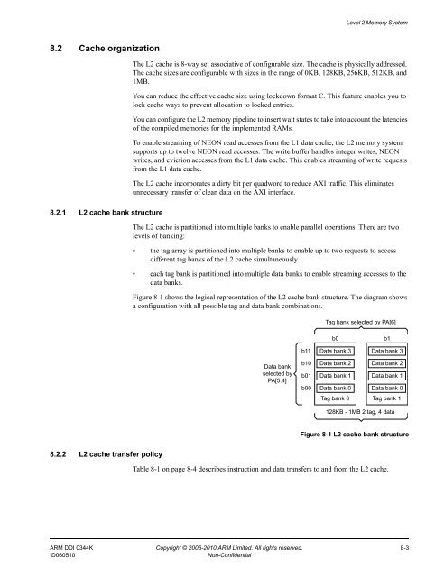
- Page 253: Chapter 8 Level 2 Memory System Thi
- Page 257 and 258: 8.3 Enabling and disabling the L2 c
- Page 259 and 260: Level 2 Memory System Note It is en
- Page 261 and 262: Level 2 Memory System Note You must
- Page 263 and 264: Lock address : LockAddr Lock free :
- Page 265 and 266: 8.7 Parity and error correction cod
- Page 267 and 268: 9.1 About the external memory inter
- Page 269 and 270: Integer data and CP14 writes Noncac
- Page 271 and 272: 9.4 AXI data read/write transaction
- Page 273 and 274: Noncacheable, or strongly ordered,
- Page 275 and 276: Noncacheable store word Noncacheabl
- Page 277 and 278: LA Last Access External Memory Inte
- Page 279 and 280: 10.1 Clock domains 10.1.1 AXI clock
- Page 281 and 282: 10.2 Reset domains 10.2.1 Power-on
- Page 283 and 284: REFCLK (PLL input) nPORESET ARESETn
- Page 285 and 286: 10.3 Power control 10.3.1 Dynamic p
- Page 287 and 288: Clock, Reset, and Power Control the
- Page 289 and 290: ATB APB I/O clamp I/O clamp L/S = L
- Page 291 and 292: ATB APB I/O clamp I/O clamp LS = Le
- Page 293 and 294: Clock, Reset, and Power Control 3.
- Page 295 and 296: Powering up the debug and ETM domai
- Page 297 and 298: 7. Perform a normal software reset
- Page 299 and 300: Clock, Reset, and Power Control 5.
- Page 301 and 302: Chapter 11 Design for Test This cha
- Page 303 and 304: In L1 MBIST Instruction Register Fi
- Page 305 and 306:
Note Do not test the CAMBIST arrays
- Page 307 and 308:
• number of rows of the L2 data,
- Page 309 and 310:
Design for Test Not all row setting
- Page 311 and 312:
In Design for Test Figure 11-4 show
- Page 313 and 314:
Design for Test When testing the ta
- Page 315 and 316:
CLK ARESETn MBISTMODE MBISTSHIFT MB
- Page 317 and 318:
End-of-test datalog retrieval Desig
- Page 319 and 320:
Pattern N RWRXMARCH 8N Row-fast Sta
- Page 321 and 322:
4. rscan array, data_seed = invert.
- Page 323 and 324:
3. R_, W, R, decr. 4. rscan data fr
- Page 325 and 326:
• the data after pass 1 of XADDRB
- Page 327 and 328:
(1 + (2 17)) 2 17 = 4,587,520 cycle
- Page 329 and 330:
processor input ports WEXTEST WINTE
- Page 331 and 332:
Design for Test toggling during shi
- Page 333 and 334:
12.1 Debug systems 12.1.1 Debug hos
- Page 335 and 336:
12.2.3 Security extensions and debu
- Page 337 and 338:
Instruction Mnemonic Description 12
- Page 339 and 340:
12.3.6 Power domains and debug 12.3
- Page 341 and 342:
Table 12-5 shows the APB interface
- Page 343 and 344:
12.4 Debug register descriptions Te
- Page 345 and 346:
MRC p14, 0, , c0, c0, 0 ; Read Debu
- Page 347 and 348:
31 30 29 28 27 26 25 24 23 22 21 20
- Page 349 and 350:
Bits Field Function [21:20] DTR acc
- Page 351 and 352:
Bits Field Function To access the D
- Page 353 and 354:
12.4.7 Watchpoint Fault Address Reg
- Page 355 and 356:
Bits Access Normal address [2] RW V
- Page 357 and 358:
12.4.12 Debug Run Control Register
- Page 359 and 360:
Table 12-23 shows how the bit value
- Page 361 and 362:
BVR[22:20] Meaning b011 The corresp
- Page 363 and 364:
Bits Field Function [15:14] Secure
- Page 365 and 366:
12.4.18 Operating System Lock Statu
- Page 367 and 368:
Debug • The sequence can be aband
- Page 369 and 370:
12.5 Management registers Offset Th
- Page 371 and 372:
Offset Register number Mnemonic Fun
- Page 373 and 374:
Bits Field Function [5] nDMAIRQ nDM
- Page 375 and 376:
12.5.7 Claim Tag Clear Register 12.
- Page 377 and 378:
12.5.10 Authentication Status Regis
- Page 379 and 380:
Table 12-45 shows fields that are i
- Page 381 and 382:
12.6 Debug events 12.6.1 Software d
- Page 383 and 384:
12.6.5 Watchpoint debug events If a
- Page 385 and 386:
Table 12-53 shows the values in the
- Page 387 and 388:
12.8 Debug state 12.8.1 Entering de
- Page 389 and 390:
12.8.4 Writing to the CPSR in debug
- Page 391 and 392:
Mode SCR[0] For CP15 instructions,
- Page 393 and 394:
12.8.9 Leaving debug state Imprecis
- Page 395 and 396:
12.9.3 Cache usage profiling Debug
- Page 397 and 398:
Note DBGPWRDWNREQ must be tied LOW
- Page 399 and 400:
If software running on the processo
- Page 401 and 402:
Rules for accessing the DCC At the
- Page 403 and 404:
} While the processor is running, i
- Page 405 and 406:
Debug Table 12-59 Values to write t
- Page 407 and 408:
12.11.4 Debug state entry Example 1
- Page 409 and 410:
} // Step 1. Update the CPSR value
- Page 411 and 412:
Writing the CPSR in debug state Exa
- Page 413 and 414:
Debug Example 12-21 Reading a word
- Page 415 and 416:
} // Step 9. Check for aborts. abor
- Page 417 and 418:
12.12 Debugging systems with energy
- Page 419 and 420:
MOV r0, r4 POP {r4, pc} Example 12-
- Page 421 and 422:
Chapter 13 NEON and VFP Programmers
- Page 423 and 424:
13.2 General-purpose registers 13.2
- Page 425 and 426:
13.3 Short vectors 13.3.1 About reg
- Page 427 and 428:
13.3.2 Operations using register ba
- Page 429 and 430:
NEON and VFP Programmers Model The
- Page 431 and 432:
Note All hardware ID information is
- Page 433 and 434:
Bits Field Function [12:8] - Reserv
- Page 435 and 436:
NEON and VFP Programmers Model Tabl
- Page 437 and 438:
13.6 Compliance with the IEEE 754 s
- Page 439 and 440:
Underflow NEON and VFP Programmers
- Page 441 and 442:
14.1 About the ETM 14.1.1 ETM featu
- Page 443 and 444:
14.1.3 NEON Bridge and bus matrix A
- Page 445 and 446:
14.3 ETM register summary The ETM r
- Page 447 and 448:
Bits Field Function [11:8] Major ET
- Page 449 and 450:
14.4.4 Peripheral Identification Re
- Page 451 and 452:
See the ETM Architecture Specificat
- Page 453 and 454:
Embedded Trace Macrocell Table 14-1
- Page 455 and 456:
Embedded Trace Macrocell Table 14-1
- Page 457 and 458:
14.5.3 Enabling events 14.5.4 Addre
- Page 459 and 460:
14.7 Context ID tracing Embedded Tr
- Page 461 and 462:
14.9 Idle state control Embedded Tr
- Page 463 and 464:
Embedded Trace Macrocell Table 14-1
- Page 465 and 466:
Chapter 15 Cross Trigger Interface
- Page 467 and 468:
CTICHIN[0] CTICHIN[1] CTICHIN[2] CT
- Page 469 and 470:
15.2 Trigger inputs and outputs Tri
- Page 471 and 472:
15.3 Connecting asynchronous channe
- Page 473 and 474:
15.5 CTI register summary Address o
- Page 475 and 476:
15.6 CTI register descriptions This
- Page 477 and 478:
15.6.4 CTI Application Trigger Clea
- Page 479 and 480:
Table 15-10 shows how the bit value
- Page 481 and 482:
15.6.12 ASIC Control Register, ASIC
- Page 483 and 484:
15.7 CTI Integration Test Registers
- Page 485 and 486:
15.7.4 ITTRIGOUTACK, 0xEF0 15.7.5 I
- Page 487 and 488:
Cross Trigger Interface Table 15-26
- Page 489 and 490:
15.8.3 Device Type Identifier, 0xFC
- Page 491 and 492:
Cross Trigger Interface Table 15-31
- Page 493 and 494:
16.1 About instruction cycle timing
- Page 495 and 496:
Instruction Cycle Timing Example 16
- Page 497 and 498:
Table 16-4 shows the operation of m
- Page 499 and 500:
Table 16-9 shows the operation of l
- Page 501 and 502:
d. See Load/store instructions on p
- Page 503 and 504:
Instruction Cycle Timing Table 16-1
- Page 505 and 506:
16.4 Other pipeline-dependent laten
- Page 507 and 508:
16.4.5 Conditional instructions Ins
- Page 509 and 510:
16.6 Instruction-specific schedulin
- Page 511 and 512:
Instruction Cycle Timing VNEG Dd,Dm
- Page 513 and 514:
VMLA a VMLS a VMLAa VMLSa VQDMLAa V
- Page 515 and 516:
VSLI VSRI 16.6.5 Advanced SIMD floa
- Page 517 and 518:
16.6.6 Advanced SIMD byte permute i
- Page 519 and 520:
Instruction Table 16-23 shows the o
- Page 521 and 522:
Instruction VST3 3-reg (unaligned)
- Page 523 and 524:
Instruction VLD3 3-reg (unaligned)
- Page 525 and 526:
Instruction Single precision cycles
- Page 527 and 528:
• FMACS, FNMACS • FMSCS, FNMSCS
- Page 529 and 530:
is dual issued with previous instru
- Page 531 and 532:
17.1 About setup and hold times AC
- Page 533 and 534:
17.2 AXI interface Table 17-2 shows
- Page 535 and 536:
17.3 ATB and CTI interfaces Table 1
- Page 537 and 538:
AC Characteristics Table 17-4 Timin
- Page 539 and 540:
17.6 L2 preload interface AC Charac
- Page 541 and 542:
17.8 Miscellaneous signals AC Chara
- Page 543 and 544:
A.1 AXI interface Signal Descriptio
- Page 545 and 546:
A.3 MBIST and DFT interface A.3.1 M
- Page 547 and 548:
A.4 Preload engine interface Table
- Page 549 and 550:
A.6 Miscellaneous signals Table A-7
- Page 551 and 552:
Signal I/O Reset Description CFGNMF
- Page 553 and 554:
Signal I/O Reset Description DBGNOP
- Page 555 and 556:
Appendix B Instruction Mnemonics Th
- Page 557 and 558:
Instruction Mnemonics Table B-1 Adv
- Page 559 and 560:
Appendix C Revisions This appendix
- Page 561 and 562:
Revisions Added text to clarify des
- Page 563 and 564:
Glossary This glossary describes so
- Page 565 and 566:
Glossary Automatic Test Pattern Gen
- Page 567 and 568:
Big-endian memory Memory in which:
- Page 569 and 570:
Conditional execution Glossary incl
- Page 571 and 572:
Glossary Embedded Trace Macrocell (
- Page 573 and 574:
Illegal instruction An instruction
- Page 575 and 576:
Glossary NaN Not a number. A symbol
- Page 577 and 578:
Glossary Significand The component
- Page 579 and 580:
Glossary Watchpoint A watchpoint is