- Page 1 and 2:
Cortex -A8Revision: r2p2Technical R
- Page 3 and 4:
Product StatusThe information in th
- Page 5 and 6:
ContentsCortex-A8 Technical Referen
- Page 7 and 8:
Contents7.8 Parity detection ......
- Page 9 and 10:
ContentsA.2 ATB interface .........
- Page 11 and 12:
List of TablesCortex-A8 Technical R
- Page 14 and 15:
List of TablesTable 3-103 Results o
- Page 16 and 17:
List of TablesTable 12-1 Access to
- Page 18 and 19:
List of TablesTable 15-3 CTI regist
- Page 20 and 21:
List of Tablesxx Copyright © 2006-
- Page 22 and 23:
List of FiguresFigure 3-10 Memory M
- Page 24 and 25:
List of FiguresFigure 10-13 Retenti
- Page 26 and 27:
List of FiguresFigure 15-16 CTI Cha
- Page 28 and 29:
PrefaceAbout this manualThis is the
- Page 30 and 31:
PrefaceChapter 16 Instruction Cycle
- Page 32 and 33:
PrefacePrefix CPrefix HPrefix nPref
- Page 34 and 35:
PrefaceFeedbackARM welcomes feedbac
- Page 36 and 37:
Introduction1.1 About the processor
- Page 38 and 39:
Introduction1.3 Components of the p
- Page 40 and 41:
Introduction1.3.4 Load/storeThe loa
- Page 42 and 43:
Introduction1.4 External interfaces
- Page 44 and 45:
Introduction1.6 Power managementThe
- Page 46 and 47:
Introduction1.8 Product revisionsTh
- Page 48 and 49:
Introduction1-14 Copyright © 2006-
- Page 50 and 51:
Programmer’s Model• Hardware co
- Page 52 and 53: Programmer’s Model2.2 Thumb-2 ins
- Page 54 and 55: Programmer’s Model2.3 ThumbEE ins
- Page 56 and 57: Programmer’s ModelThumbEE Handler
- Page 58 and 59: Programmer’s Model2.4 Jazelle Ext
- Page 60 and 61: Programmer’s Model— the registe
- Page 62 and 63: Programmer’s ModelNonsecureSecure
- Page 64 and 65: Programmer’s Model2.7 VFPv3 archi
- Page 66 and 67: Programmer’s Model2.9 Data typesT
- Page 68 and 69: Programmer’s ModelBitHigher addre
- Page 70 and 71: Programmer’s Model2.12 Operating
- Page 72 and 73: Programmer’s ModelIn privileged m
- Page 74 and 75: Programmer’s Model16 generalpurpo
- Page 76 and 77: Programmer’s ModelIn ARM state, y
- Page 78 and 79: Programmer’s Model2.14.5 The GE[3
- Page 80 and 81: Programmer’s ModelT bitThe T bit
- Page 82 and 83: Programmer’s ModelOnly secure pri
- Page 84 and 85: Programmer’s Model2.15.2 Leaving
- Page 86 and 87: Programmer’s ModelAn internal or
- Page 88 and 89: Programmer’s ModelImprecise data
- Page 90 and 91: Programmer’s ModelNoteIf the Embe
- Page 92 and 93: Programmer’s Model2.16 Software c
- Page 94 and 95: Programmer’s Model2.17.2 Security
- Page 96 and 97: Programmer’s Model2.18 Control co
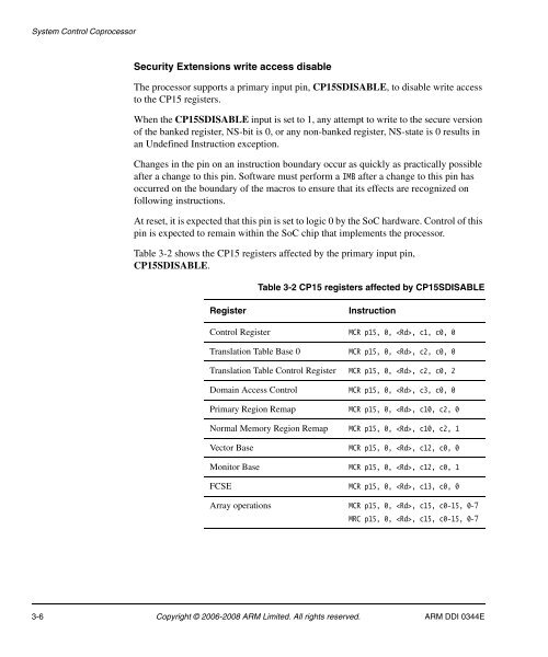
- Page 98 and 99: System Control Coprocessor3.1 About
- Page 100 and 101: System Control CoprocessorTable 3-1
- Page 104 and 105: System Control Coprocessor3.1.6 Sys
- Page 106 and 107: System Control CoprocessorTable 3-3
- Page 108 and 109: System Control CoprocessorTable 3-3
- Page 110 and 111: System Control CoprocessorTable 3-3
- Page 112 and 113: System Control CoprocessorTable 3-3
- Page 114 and 115: System Control CoprocessorTable 3-3
- Page 116 and 117: System Control CoprocessorTable 3-3
- Page 118 and 119: System Control CoprocessorTable 3-3
- Page 120 and 121: System Control CoprocessorTable 3-3
- Page 122 and 123: System Control CoprocessorTable 3-5
- Page 124 and 125: System Control CoprocessorThe TCM T
- Page 126 and 127: System Control CoprocessorTable 3-1
- Page 128 and 129: System Control CoprocessorFigure 3-
- Page 130 and 131: System Control CoprocessorTable 3-1
- Page 132 and 133: System Control CoprocessorTable 3-1
- Page 134 and 135: System Control CoprocessorTable 3-2
- Page 136 and 137: System Control CoprocessorTable 3-2
- Page 138 and 139: System Control Coprocessor31 28 27
- Page 140 and 141: System Control CoprocessorTable 3-2
- Page 142 and 143: System Control CoprocessorTable 3-3
- Page 144 and 145: System Control CoprocessorTable 3-3
- Page 146 and 147: System Control CoprocessorTable 3-3
- Page 148 and 149: System Control Coprocessor3.2.20 c0
- Page 150 and 151: System Control Coprocessor31 24 23
- Page 152 and 153:
System Control CoprocessorTable 3-4
- Page 154 and 155:
System Control Coprocessora. An ent
- Page 156 and 157:
System Control CoprocessorTable 3-4
- Page 158 and 159:
System Control CoprocessorThe Auxil
- Page 160 and 161:
System Control CoprocessorBits Fiel
- Page 162 and 163:
System Control CoprocessorBits Fiel
- Page 164 and 165:
System Control Coprocessora. n is t
- Page 166 and 167:
System Control CoprocessorTable 3-5
- Page 168 and 169:
System Control CoprocessorFigure 3-
- Page 170 and 171:
System Control CoprocessorBits Fiel
- Page 172 and 173:
System Control CoprocessorBits Fiel
- Page 174 and 175:
System Control CoprocessorBits Fiel
- Page 176 and 177:
System Control CoprocessorTable 3-6
- Page 178:
System Control CoprocessorBits Fiel
- Page 181 and 182:
System Control CoprocessorMRC p15,
- Page 183 and 184:
System Control Coprocessor3.2.37 c5
- Page 185 and 186:
System Control CoprocessorTable 3-7
- Page 187 and 188:
System Control CoprocessorTable 3-7
- Page 189 and 190:
System Control CoprocessorTable 3-7
- Page 191 and 192:
System Control CoprocessorTable 3-7
- Page 193 and 194:
System Control CoprocessorVA to PA
- Page 195 and 196:
System Control CoprocessorTable 3-8
- Page 197 and 198:
System Control CoprocessorInvalidat
- Page 199 and 200:
System Control CoprocessorThe PMNC
- Page 201 and 202:
System Control CoprocessorCWhen wri
- Page 203 and 204:
System Control CoprocessorTable 3-8
- Page 205 and 206:
System Control Coprocessor3.2.47 c9
- Page 207 and 208:
System Control CoprocessorMRC p15,
- Page 209 and 210:
System Control CoprocessorTable 3-9
- Page 211 and 212:
System Control CoprocessorTable 3-9
- Page 213 and 214:
System Control Coprocessorb. The EN
- Page 215 and 216:
System Control CoprocessorCWhen rea
- Page 217 and 218:
System Control CoprocessorTable 3-1
- Page 219 and 220:
System Control CoprocessorTable 3-1
- Page 221 and 222:
System Control Coprocessor• acces
- Page 223 and 224:
System Control CoprocessorBits Fiel
- Page 225 and 226:
System Control CoprocessorYou can c
- Page 227 and 228:
System Control CoprocessorIf the op
- Page 229 and 230:
System Control Coprocessor31 20 19
- Page 231 and 232:
System Control CoprocessorTable 3-1
- Page 233 and 234:
System Control CoprocessorTo access
- Page 235 and 236:
System Control CoprocessorTable 3-1
- Page 237 and 238:
System Control Coprocessora. An ent
- Page 239 and 240:
System Control Coprocessor3.2.62 c1
- Page 241 and 242:
System Control CoprocessorTable 3-1
- Page 243 and 244:
System Control CoprocessorTo access
- Page 245 and 246:
System Control CoprocessorThe PLE I
- Page 247 and 248:
System Control CoprocessorTable 3-1
- Page 249 and 250:
System Control CoprocessorTable 3-1
- Page 251 and 252:
System Control CoprocessorTable 3-1
- Page 253 and 254:
System Control CoprocessorMRC p15,
- Page 255 and 256:
System Control Coprocessor31 25 24
- Page 257 and 258:
System Control Coprocessor3.2.72 c1
- Page 259 and 260:
System Control CoprocessorTable 3-1
- Page 261 and 262:
System Control CoprocessorFigure 3-
- Page 263 and 264:
System Control CoprocessorTo perfor
- Page 265 and 266:
System Control Coprocessor3.2.75 c1
- Page 267 and 268:
System Control CoprocessorLDR R1, =
- Page 269 and 270:
System Control CoprocessorLDR R1, =
- Page 271 and 272:
System Control CoprocessorL1 Data 0
- Page 273 and 274:
System Control CoprocessorInstructi
- Page 275 and 276:
System Control CoprocessorParity/EC
- Page 277 and 278:
System Control CoprocessorTable 3-1
- Page 279 and 280:
System Control CoprocessorL2 parity
- Page 281 and 282:
System Control CoprocessorThe L2 da
- Page 283 and 284:
Chapter 4Unaligned Data and Mixed-e
- Page 285 and 286:
Unaligned Data and Mixed-endian Dat
- Page 287 and 288:
Unaligned Data and Mixed-endian Dat
- Page 289 and 290:
Chapter 5Program Flow PredictionThi
- Page 291 and 292:
Program Flow Prediction5.2 Predicte
- Page 293 and 294:
Program Flow Prediction5.2.1 Return
- Page 295 and 296:
Program Flow Prediction5.4 Guidelin
- Page 297 and 298:
Program Flow Prediction5.6 Operatin
- Page 299 and 300:
Chapter 6Memory Management UnitThis
- Page 301 and 302:
Memory Management Unit6.2 Memory ac
- Page 303 and 304:
Memory Management Unit6.4 MMU inter
- Page 305 and 306:
Memory Management Unit6.6 TLB lockd
- Page 307 and 308:
Chapter 7Level 1 Memory SystemThis
- Page 309 and 310:
Level 1 Memory System7.2 Cache orga
- Page 311 and 312:
Level 1 Memory System7.3 Memory att
- Page 313 and 314:
Level 1 Memory SystemTable 7-1 Memo
- Page 315 and 316:
Level 1 Memory System7.5 Data cache
- Page 317 and 318:
Level 1 Memory SystemAn exception t
- Page 319 and 320:
Level 1 Memory System7.8 Parity det
- Page 321 and 322:
Chapter 8Level 2 Memory SystemThis
- Page 323 and 324:
Level 2 Memory System8.2 Cache orga
- Page 325 and 326:
Level 2 Memory System8.3 Enabling a
- Page 327 and 328:
Level 2 Memory SystemControl Regist
- Page 329 and 330:
Level 2 Memory System8.4.4 Memory r
- Page 331 and 332:
Level 2 Memory System8.5 Synchroniz
- Page 333 and 334:
Level 2 Memory System8.6 Locked acc
- Page 335 and 336:
Chapter 9External Memory InterfaceT
- Page 337 and 338:
External Memory Interfaceto the wri
- Page 339 and 340:
External Memory InterfaceTable 9-2
- Page 341 and 342:
External Memory Interface9.3 AXI in
- Page 343 and 344:
External Memory InterfaceBWBCNoTTSS
- Page 345 and 346:
External Memory InterfaceTable 9-6
- Page 347 and 348:
External Memory InterfaceTable 9-6
- Page 349 and 350:
External Memory InterfaceTable 9-6
- Page 351 and 352:
External Memory InterfaceTable 9-7
- Page 353 and 354:
Chapter 10Clock, Reset, and Power C
- Page 355 and 356:
Clock, Reset, and Power Controlfami
- Page 357 and 358:
Clock, Reset, and Power Control10.2
- Page 359 and 360:
Clock, Reset, and Power Control•
- Page 361 and 362:
Clock, Reset, and Power Control2. F
- Page 363 and 364:
Clock, Reset, and Power ControlNote
- Page 365 and 366:
Clock, Reset, and Power ControlAfte
- Page 367 and 368:
Clock, Reset, and Power Control•
- Page 369 and 370:
Clock, Reset, and Power Control—
- Page 371 and 372:
Clock, Reset, and Power ControlThe
- Page 373 and 374:
Clock, Reset, and Power ControlPowe
- Page 375 and 376:
Clock, Reset, and Power ControlTo p
- Page 377 and 378:
Clock, Reset, and Power ControlPowe
- Page 379 and 380:
Clock, Reset, and Power ControlATBI
- Page 381 and 382:
Clock, Reset, and Power Control7. P
- Page 383 and 384:
Chapter 11Design for TestThis chapt
- Page 385 and 386:
Design for Test11.1.2 MBIST registe
- Page 387 and 388:
Design for Testdseed[3:0]Write the
- Page 389 and 390:
Design for TestNoteOnly arrays with
- Page 391 and 392:
Design for Test• read and write l
- Page 393 and 394:
Design for TestTable 11-10 Selectin
- Page 395 and 396:
Design for TestTable 11-15 shows ho
- Page 397 and 398:
Design for TestArrayFail[22:0] fail
- Page 399 and 400:
Design for TestWhen testing the tag
- Page 401 and 402:
Design for Test• Bitmap test mode
- Page 403 and 404:
Design for TestCLKARESETnMBISTMODEM
- Page 405 and 406:
Design for TestCLKARESETnMBISTMODEM
- Page 407 and 408:
Design for TestTable 11-19 shows th
- Page 409 and 410:
Design for TestNoteNormal MBIST tes
- Page 411 and 412:
Design for TestRowmaxmax - 11 1 1 1
- Page 413 and 414:
Design for Test2. R, W_, R_, incr.3
- Page 415 and 416:
Design for TestRow3210Addressingdir
- Page 417 and 418:
Design for TestRow32100 00 00 00 00
- Page 419 and 420:
Design for Test11.2 ATPG test featu
- Page 421 and 422:
Design for TestWBR in place of the
- Page 423 and 424:
Design for TestOne methodology for
- Page 425 and 426:
Chapter 12DebugThis chapter describ
- Page 427 and 428:
Debug12.1.3 Debug targetThe debug t
- Page 429 and 430:
DebugWhen execution of a monitor ta
- Page 431 and 432:
Debug12.3 Debug register interfaceY
- Page 433 and 434:
DebugTable 12-3 Debug memory-mapped
- Page 435 and 436:
Debug12.3.6 Power domains and debug
- Page 437 and 438:
DebugLocks permissionYou can lock t
- Page 439 and 440:
DebugTable 12-6 shows the behavior
- Page 441 and 442:
Debug12.4 Debug register descriptio
- Page 443 and 444:
DebugTable 12-11 shows how the bit
- Page 445 and 446:
DebugThe Debug Self Address Offset
- Page 447 and 448:
DebugBits Field FunctionTable 12-14
- Page 449 and 450:
DebugBits Field FunctionTable 12-14
- Page 451 and 452:
DebugBits Field Function[9] - Reser
- Page 453 and 454:
DebugThe DTR access mode can be one
- Page 455 and 456:
DebugBitsFieldFunctionTable 12-16 s
- Page 457 and 458:
DebugTable 12-17 Vector Catch Regis
- Page 459 and 460:
Debug31 3 2 1 0ReservedNot write-th
- Page 461 and 462:
DebugBits Field FunctionTable 12-21
- Page 463 and 464:
DebugBits Field FunctionTable 12-23
- Page 465 and 466:
DebugTable 12-23 Breakpoint Control
- Page 467 and 468:
Debug12.4.16 Watchpoint Control Reg
- Page 469 and 470:
DebugTable 12-26 Watchpoint Control
- Page 471 and 472:
DebugBits Field FunctionTable 12-27
- Page 473 and 474:
DebugBits Field FunctionTable 12-29
- Page 475 and 476:
DebugBits Field FunctionTable 12-30
- Page 477 and 478:
DebugNoteOn system reset, PRSR[1] r
- Page 479 and 480:
DebugTable 12-32 Management registe
- Page 481 and 482:
DebugFigure 12-19 shows the bit arr
- Page 483 and 484:
DebugBits Field FunctionTable 12-35
- Page 485 and 486:
Debug12.5.5 Integration Mode Contro
- Page 487 and 488:
Debug12.5.8 Lock Access RegisterThe
- Page 489 and 490:
Debug31 8 7 6 5 4 3 2 1 0ReservedSe
- Page 491 and 492:
DebugTable 12-44 Peripheral Identif
- Page 493 and 494:
DebugTable 12-50 shows how the bit
- Page 495 and 496:
Debug12.6.2 Halting debug event•
- Page 497 and 498:
Debug12.6.5 Watchpoint debug events
- Page 499 and 500:
DebugNoteThe Data Abort handler che
- Page 501 and 502:
DebugIf the debugged code is not ru
- Page 503 and 504:
DebugTable 12-54 shows the read PC
- Page 505 and 506:
Debug12.8.4 Writing to the CPSR in
- Page 507 and 508:
DebugCoprocessor instructionsThe ru
- Page 509 and 510:
DebugSVCSMCUndefinedThe processor i
- Page 511 and 512:
Debug12.9 Cache debugThere are seve
- Page 513 and 514:
Debug12.10 External debug interface
- Page 515 and 516:
DebugDBGROMADDRThe DBGROMADDR signa
- Page 517 and 518:
Debug4. Issue an Instruction Synchr
- Page 519 and 520:
Debug12.11.1 Debug communications c
- Page 521 and 522:
DebugDebugger access to the DCCA de
- Page 523 and 524:
DebugTable 12-58 Values to write to
- Page 525 and 526:
Debug}when 1:byte_address_select :=
- Page 527 and 528:
DebugNoteIn Example 12-10 on page 1
- Page 529 and 530:
Debug12.11.5 Debug state exitWhen e
- Page 531 and 532:
DebugExample 12-15 Reading the PCRe
- Page 533 and 534:
DebugExample 12-19 Checking for an
- Page 535 and 536:
DebugExample 12-22 shows the sequen
- Page 537 and 538:
Debug}dscr := ReadDebugRegister(34)
- Page 539 and 540:
Debug}scr := (scr | 1);WriteCPReg(1
- Page 541 and 542:
DebugIf on a power-down request fro
- Page 543 and 544:
Debug; Step 2. Loop writing words f
- Page 545 and 546:
Chapter 13NEON and VFP Programmer
- Page 547 and 548:
NEON and VFP Programmer’s Modelre
- Page 549 and 550:
NEON and VFP Programmer’s ModelS0
- Page 551 and 552:
NEON and VFP Programmer’s ModelBa
- Page 553 and 554:
NEON and VFP Programmer’s ModelFC
- Page 555 and 556:
NEON and VFP Programmer’s ModelTa
- Page 557 and 558:
NEON and VFP Programmer’s ModelTa
- Page 559 and 560:
NEON and VFP Programmer’s Model31
- Page 561 and 562:
NEON and VFP Programmer’s ModelTh
- Page 563 and 564:
NEON and VFP Programmer’s ModelTa
- Page 565 and 566:
NEON and VFP Programmer’s Model13
- Page 567 and 568:
NEON and VFP Programmer’s Model13
- Page 569 and 570:
NEON and VFP Programmer’s ModelCo
- Page 571 and 572:
Chapter 14Embedded Trace MacrocellT
- Page 573 and 574:
Embedded Trace Macrocell14.1.2 The
- Page 575 and 576:
Embedded Trace Macrocell(DAP) throu
- Page 577 and 578:
Embedded Trace MacrocellTable 14-1
- Page 579 and 580:
Embedded Trace MacrocellRegister na
- Page 581 and 582:
Embedded Trace MacrocellTable 14-3
- Page 583 and 584:
Embedded Trace MacrocellTable 14-4
- Page 585 and 586:
Embedded Trace MacrocellTable 14-6
- Page 587 and 588:
Embedded Trace MacrocellSee the ETM
- Page 589 and 590:
Embedded Trace MacrocellTable 14-11
- Page 591 and 592:
Embedded Trace MacrocellTable 14-14
- Page 593 and 594:
Embedded Trace Macrocell14.5 Precis
- Page 595 and 596:
Embedded Trace MacrocellThe followi
- Page 597 and 598:
Embedded Trace Macrocellcomparator
- Page 599 and 600:
Embedded Trace Macrocell14.8 Instru
- Page 601 and 602:
Embedded Trace MacrocellWhen a WFI
- Page 603 and 604:
Embedded Trace MacrocellTable 14-17
- Page 605 and 606:
Embedded Trace MacrocellYou can use
- Page 607 and 608:
Chapter 15Cross Trigger InterfaceTh
- Page 609 and 610:
Cross Trigger Interface• An input
- Page 611 and 612:
Cross Trigger Interface15.1.2 The c
- Page 613 and 614:
Cross Trigger InterfaceTable 15-2 T
- Page 615 and 616:
Cross Trigger Interface15.4 About t
- Page 617 and 618:
Cross Trigger InterfaceTable 15-3 C
- Page 619 and 620:
Cross Trigger Interface15.6 CTI reg
- Page 621 and 622:
Cross Trigger InterfaceNoteThe CTII
- Page 623 and 624:
Cross Trigger InterfaceBits Field F
- Page 625 and 626:
Cross Trigger Interface15.6.9 CTI T
- Page 627 and 628:
Cross Trigger InterfaceTable 15-14
- Page 629 and 630:
Cross Trigger InterfaceTable 15-16
- Page 631 and 632:
Cross Trigger InterfaceTable 15-18
- Page 633 and 634:
Cross Trigger Interface15.7.4 ITTRI
- Page 635 and 636:
Cross Trigger InterfaceTable 15-26
- Page 637 and 638:
Cross Trigger Interface15.8.3 Devic
- Page 639 and 640:
Cross Trigger InterfaceActual Compo
- Page 641 and 642:
Chapter 16Instruction Cycle TimingT
- Page 643 and 644:
Instruction Cycle Timing16.2 Instru
- Page 645 and 646:
Instruction Cycle Timingis availabl
- Page 647 and 648:
Instruction Cycle TimingTable 16-4
- Page 649 and 650:
Instruction Cycle Timing16.2.7 Stat
- Page 651 and 652:
Instruction Cycle TimingThe number
- Page 653 and 654:
Instruction Cycle Timing16.3 Dual-i
- Page 655 and 656:
Instruction Cycle TimingReplayevent
- Page 657 and 658:
Instruction Cycle TimingPredicting
- Page 659 and 660:
Instruction Cycle TimingUsing MCR i
- Page 661 and 662:
Instruction Cycle TimingExample 16-
- Page 663 and 664:
Instruction Cycle TimingTable 16-15
- Page 665 and 666:
Instruction Cycle Timing16.6.3 Adva
- Page 667 and 668:
Instruction Cycle TimingTable 16-16
- Page 669 and 670:
Instruction Cycle Timing16.6.5 Adva
- Page 671 and 672:
Instruction Cycle TimingTable 16-19
- Page 673 and 674:
Instruction Cycle TimingFor example
- Page 675 and 676:
Instruction Cycle TimingTable 16-20
- Page 677 and 678:
Instruction Cycle TimingTable 16-20
- Page 679 and 680:
Instruction Cycle TimingTable 16-20
- Page 681 and 682:
Instruction Cycle Timing16.7 VFP in
- Page 683 and 684:
Instruction Cycle TimingTable 16-22
- Page 685 and 686:
Instruction Cycle Timing16.7.2 VFP
- Page 687 and 688:
Chapter 17AC CharacteristicsThis ch
- Page 689 and 690:
AC CharacteristicsThe timing parame
- Page 691 and 692:
AC CharacteristicsTable 17-2 Timing
- Page 693 and 694:
AC Characteristics17.4 APB interfac
- Page 695 and 696:
AC Characteristics17.5 L1 and L2 MB
- Page 697 and 698:
AC Characteristics17.7 DFT interfac
- Page 699 and 700:
AC Characteristicsb. Figure 10-6 on
- Page 701 and 702:
Appendix ASignal DescriptionsThis a
- Page 703 and 704:
Signal DescriptionsA.2 ATB interfac
- Page 705 and 706:
Signal DescriptionsTable A-3 MBIST
- Page 707 and 708:
Signal DescriptionsA.4 Preload engi
- Page 709 and 710:
Signal DescriptionsTable A-6 APB in
- Page 711 and 712:
Signal DescriptionsTable A-7 Miscel
- Page 713 and 714:
Signal DescriptionsTable A-7 Miscel
- Page 715 and 716:
Signal DescriptionsTable A-8 Miscel
- Page 717 and 718:
Signal DescriptionsA.8 Miscellaneou
- Page 719 and 720:
Appendix BInstruction MnemonicsThis
- Page 721 and 722:
Instruction MnemonicsTable B-1 Adva
- Page 723 and 724:
Instruction MnemonicsB.2 VFP data-p
- Page 725 and 726:
GlossaryThis glossary describes som
- Page 727 and 728:
GlossaryApplication Specific Integr
- Page 729 and 730:
GlossaryRead ID capabilityThe maxim
- Page 731 and 732:
GlossaryByte-invariantIn a byte-inv
- Page 733 and 734:
GlossaryCAM includes comparison log
- Page 735 and 736:
GlossaryDouble-precision valueConsi
- Page 737 and 738:
Glossary• arithmetic operation re
- Page 739 and 740:
GlossaryInvalidateJazelle architect
- Page 741 and 742:
GlossaryPAPenaltyPower-on resetPref
- Page 743 and 744:
GlossarySetSet-associative cacheSee
- Page 745 and 746:
GlossaryTrapTrigger instructionAn e
- Page 747 and 748:
GlossaryWrite-back (WB)Write buffer