- Page 1 and 2:
®ARM®Cortex -A15 MPCoreProcessorR
- Page 3 and 4:
ContentsARM Cortex-A15 MPCore Proce
- Page 5 and 6:
Contents11.4 PMU register descripti
- Page 7 and 8:
PrefaceAbout this bookThis book is
- Page 9 and 10:
Preface(continued)Stylemonospace bo
- Page 11 and 12:
PrefaceFeedbackARM welcomes feedbac
- Page 13 and 14:
Introduction1.1 About the Cortex-A1
- Page 15 and 16:
Introduction1.2.3 Debug architectur
- Page 17 and 18:
Introduction1.4 InterfacesThe proce
- Page 19 and 20:
Introduction• The L2 tag RAM regi
- Page 21 and 22:
IntroductionThe ARM product deliver
- Page 23 and 24:
Introduction1.7.5 r1p0 - r2p0The fo
- Page 25 and 26:
Introduction• Added L1 data TLB s
- Page 27 and 28:
Functional Description2.1 About the
- Page 29 and 30:
Functional DescriptionLoad/Store un
- Page 31 and 32:
Functional Description2.2 Interface
- Page 33 and 34:
Functional Description2.3 Clocking
- Page 35 and 36:
Functional DescriptionFigure 2-5 sh
- Page 37:
Functional DescriptionAll resets ar
- Page 41 and 42: Functional DescriptionPowerup reset
- Page 43 and 44: Functional Description• nPRESETDB
- Page 45 and 46: Functional Description• L2 unifie
- Page 47 and 48: Functional DescriptionOn entry into
- Page 49 and 50: Functional DescriptionWhen the proc
- Page 51 and 52: Functional DescriptionNoteFigure 2-
- Page 53 and 54: Functional DescriptionRegional cloc
- Page 55 and 56: Functional DescriptionTable 2-3 Val
- Page 57 and 58: Functional Description4. Release th
- Page 59 and 60: Functional DescriptionDebug power d
- Page 61 and 62: Functional DescriptionNoteAfter a p
- Page 63 and 64: Functional DescriptionThe external
- Page 65 and 66: Programmers Model3.1 About the prog
- Page 67 and 68: Programmers Model3.3 Advanced SIMD
- Page 69 and 70: Programmers ModelYou can use the CP
- Page 71 and 72: Programmers Model3.6 Large Physical
- Page 73 and 74: Programmers Model3.8 Modes of opera
- Page 75 and 76: Chapter 4System ControlThis chapter
- Page 77 and 78: System Control4.2 Register summaryT
- Page 79 and 80: System ControlOp1 CRm Op2 Name Rese
- Page 81 and 82: System ControlTable 4-6 c5 register
- Page 83 and 84: System ControlTable 4-8 c7 register
- Page 85 and 86: System ControlTable 4-10 c9 registe
- Page 87 and 88: System Control4.2.14 c15 registersT
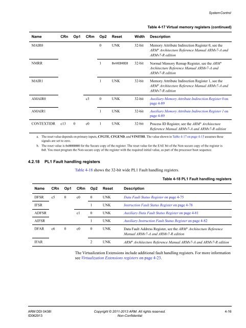
- Page 89: System ControlName CRn Op1 CRm Op2
- Page 93 and 94: System ControlName CRn Op1 CRm Op2
- Page 95 and 96: System Control4.2.24 Performance mo
- Page 97 and 98: System Control4.2.26 Virtualization
- Page 99 and 100: System ControlName CRn Op1 CRm Op2
- Page 101 and 102: System Control4.3 Register descript
- Page 103 and 104: System ControlTo access the CTR, re
- Page 106 and 107: System ControlTable 4-34 shows the
- Page 108 and 109: System ControlTable 4-36 shows the
- Page 110 and 111: System Control4.3.12 Memory Model F
- Page 112 and 113: System ControlTable 4-39 shows the
- Page 114 and 115: System ControlTable 4-40 ID_MMFR3 b
- Page 116 and 117: System Control31 28 27 24 23 20 19
- Page 118 and 119: System ControlTable 4-43 ID_ISAR2 b
- Page 120 and 121: System ControlTable 4-44 ID_ISAR3 b
- Page 122 and 123: System ControlTable 4-45 ID_ISAR4 b
- Page 124 and 125: System ControlTable 4-47 shows the
- Page 126 and 127: System ControlConfigurationsAvailab
- Page 128 and 129: System ControlMCR p15, 4, , c0, c0,
- Page 130 and 131: System ControlTable 4-52 SCTLR bit
- Page 132 and 133: System Control31 30 29 28 27 26 25
- Page 134 and 135: System ControlTable 4-53 ACTLR bit
- Page 136 and 137: System ControlTable 4-53 ACTLR bit
- Page 138 and 139: System ControlUsage constraints The
- Page 140 and 141:
System Control• The L2 internal a
- Page 142 and 143:
System Control31 30 29 28 27 26 25
- Page 144 and 145:
System ControlTable 4-58 shows the
- Page 146 and 147:
System ControlUsage constraints The
- Page 148 and 149:
System ControlTable 4-59 HCPTR bit
- Page 150 and 151:
System ControlTable 4-60 shows the
- Page 152 and 153:
System ControlTable 4-61 DFSR bit a
- Page 154 and 155:
System ControlTable 4-63 IFSR bit a
- Page 156 and 157:
System ControlConfigurationsAvailab
- Page 158 and 159:
System Control• UNKNOWN when exec
- Page 160 and 161:
System Control31 30 26 25 24 23 22
- Page 162 and 163:
System Control• Only accessible f
- Page 164 and 165:
System Control31 0DataFigure 4-40 I
- Page 166 and 167:
System ControlTable 4-73 shows the
- Page 168 and 169:
System ControlThe data returned fro
- Page 170 and 171:
System ControlThe data returned fro
- Page 172 and 173:
System Control31 24 23 21 20 19 18
- Page 174 and 175:
System Control4.3.60 L2 Auxiliary C
- Page 176 and 177:
System ControlTable 4-74 L2ACTLR bi
- Page 178 and 179:
System Control• Is only accessibl
- Page 180 and 181:
System ControlTable 4-76 shows the
- Page 182 and 183:
System ControlTable 4-78 shows the
- Page 184 and 185:
System ControlTable 4-79 L2MERRSR b
- Page 186 and 187:
Memory Management Unit5.1 About the
- Page 188 and 189:
Memory Management Unit5.3 TLB match
- Page 190 and 191:
Memory Management Unit• The TLB t
- Page 192 and 193:
Memory Management Unit5.6 Intermedi
- Page 194 and 195:
Memory Management Unit5.7 External
- Page 196 and 197:
Level 1 Memory System6.1 About the
- Page 198 and 199:
Level 1 Memory System6.3 L1 instruc
- Page 200 and 201:
Level 1 Memory System6.4 L1 data me
- Page 202 and 203:
Level 1 Memory SystemL1 or L2 cache
- Page 204 and 205:
Level 1 Memory SystemExternal globa
- Page 206 and 207:
Level 1 Memory System6.5 Program fl
- Page 208 and 209:
Level 1 Memory SystemReset:• Disa
- Page 210 and 211:
Chapter 7Level 2 Memory SystemThis
- Page 212 and 213:
Level 2 Memory System7.2 Cache orga
- Page 214 and 215:
Level 2 Memory System7.2.5 Register
- Page 216 and 217:
Level 2 Memory SystemNote• The L2
- Page 218 and 219:
Level 2 Memory System7.4 L2 cache p
- Page 220 and 221:
Level 2 Memory System7.6 Asynchrono
- Page 222 and 223:
Level 2 Memory SystemFor certain tr
- Page 224 and 225:
Level 2 Memory System7.7.6 Snoop fi
- Page 226 and 227:
Level 2 Memory SystemTable 7-6 show
- Page 228 and 229:
Chapter 8Generic Interrupt Controll
- Page 230 and 231:
Generic Interrupt Controller8.2 GIC
- Page 232 and 233:
Generic Interrupt Controller8.2.4 I
- Page 234 and 235:
Generic Interrupt Controller8.3 GIC
- Page 236 and 237:
Generic Interrupt ControllerOffset
- Page 238 and 239:
Generic Interrupt ControllerTable 8
- Page 240 and 241:
Generic Interrupt ControllerPrivate
- Page 242 and 243:
Generic Interrupt Controller0x1D043
- Page 244 and 245:
Generic Interrupt ControllerThe Cor
- Page 246 and 247:
Generic Interrupt ControllerTable 8
- Page 248 and 249:
Generic Interrupt Controller8.3.8 V
- Page 250 and 251:
Generic Timer9.1 About the Generic
- Page 252 and 253:
Generic Timer9.3 Generic Timer prog
- Page 254 and 255:
Chapter 10DebugThis chapter describ
- Page 256 and 257:
Debug• Operating systems.• Hard
- Page 258 and 259:
DebugnPRESETDBGThis signal initiali
- Page 260 and 261:
DebugTable 10-1 CP14 debug register
- Page 262 and 263:
DebugTable 10-1 CP14 debug register
- Page 264 and 265:
DebugTable 10-2 DBGDIDR bit assignm
- Page 266 and 267:
DebugTable 10-4 shows the DBGDRCR b
- Page 268 and 269:
DebugConfigurationsAttributesThe pr
- Page 270 and 271:
DebugTable 10-8 DBGBCR bit assignme
- Page 272 and 273:
DebugTable 10-10 shows the DBGWCR b
- Page 274 and 275:
Debug31 12 11 2 1 0ROMADDR[31:12]Re
- Page 276 and 277:
Debug10.4.12 OS Lock Status Registe
- Page 278 and 279:
DebugTable 10-15 shows the DBGPRCR
- Page 280 and 281:
DebugTable 10-16 DBGDSAR bit assign
- Page 282 and 283:
Debug31 1 0ReservedIntegration mode
- Page 284 and 285:
DebugTable 10-22 shows the DBGDEVID
- Page 286 and 287:
Debug10.4.23 Component Identificati
- Page 288 and 289:
Debug10.6 External debug interfaceT
- Page 290 and 291:
DebugIf software running on the pro
- Page 292 and 293:
Performance Monitor Unit11.1 About
- Page 294 and 295:
Performance Monitor Unit11.3 PMU re
- Page 296 and 297:
Performance Monitor UnitTable 11-1
- Page 298 and 299:
Performance Monitor UnitTable 11-2
- Page 300 and 301:
Performance Monitor UnitTable 11-3
- Page 302 and 303:
Performance Monitor UnitTable 11-4
- Page 304 and 305:
Performance Monitor Unit11.5 Effect
- Page 306 and 307:
Performance Monitor UnitTable 11-7
- Page 308 and 309:
Performance Monitor Unit11.7 Interr
- Page 310 and 311:
Chapter 12Program Trace MacrocellTh
- Page 312 and 313:
Program Trace Macrocell12.2 PTM opt
- Page 314 and 315:
Program Trace MacrocellYou can also
- Page 316 and 317:
Program Trace Macrocell12.5 PTM pro
- Page 318 and 319:
Program Trace Macrocellarchitecture
- Page 320 and 321:
Program Trace Macrocell12.6 Registe
- Page 322 and 323:
Program Trace MacrocellTable 12-4 P
- Page 324 and 325:
Program Trace MacrocellTable 12-5 E
- Page 326 and 327:
Program Trace MacrocellTable 12-6 E
- Page 328 and 329:
Program Trace Macrocell31 26 25 24
- Page 330 and 331:
Program Trace Macrocell12.7.8 Confi
- Page 332 and 333:
Program Trace Macrocell12.7.10 Auxi
- Page 334 and 335:
Program Trace Macrocell31 4 3 2 0Re
- Page 336 and 337:
Program Trace MacrocellTable 12-17
- Page 338 and 339:
Program Trace Macrocell31 7 60Reser
- Page 340 and 341:
Program Trace MacrocellThe Componen
- Page 342 and 343:
Cross Trigger13.1 About the cross t
- Page 344 and 345:
Cross Trigger13.3 Cortex-A15 CTIIn
- Page 346 and 347:
Chapter 14NEON and VFP UnitThis cha
- Page 348 and 349:
NEON and VFP UnitARM DDI 0438I Copy
- Page 350 and 351:
NEON and VFP UnitSee the ARM ® Arc
- Page 352 and 353:
NEON and VFP UnitConfigurationsAvai
- Page 354 and 355:
NEON and VFP UnitTable 14-5 FPSCR b
- Page 356 and 357:
NEON and VFP UnitTable 14-6 MVFR1 b
- Page 358 and 359:
NEON and VFP Unit31 30 29 0Reserved
- Page 360 and 361:
Signal DescriptionsA.1 About the si
- Page 362 and 363:
Signal DescriptionsA.3 Reset signal
- Page 364 and 365:
Signal DescriptionsA.5 Generic Inte
- Page 366 and 367:
Signal DescriptionsA.6 Generic Time
- Page 368 and 369:
Signal DescriptionsA.8 Power manage
- Page 370 and 371:
Signal DescriptionsA.9 AXI interfac
- Page 372 and 373:
Signal DescriptionsWrite address ch
- Page 374 and 375:
Signal DescriptionsTable A-14 Read
- Page 376 and 377:
Signal DescriptionsTable A-20 Write
- Page 378 and 379:
Signal DescriptionsA.10 External de
- Page 380 and 381:
Signal DescriptionsTable A-27 Misce
- Page 382 and 383:
Signal DescriptionsA.12 Cross trigg
- Page 384 and 385:
Signal DescriptionsA.14 DFT and MBI
- Page 386 and 387:
Appendix BRevisionsThis appendix de
- Page 388 and 389:
RevisionsTable B-3 Differences betw
- Page 390 and 391:
RevisionsTable B-7 Differences betw
- Page 392:
RevisionsTable B-8 Differences betw


