- Page 2 and 3:
© 2002 by CRC Press LLC
- Page 6 and 7:
© 2002 by CRC Press LLC Fernanda p
- Page 8 and 9:
Locating Your Topic Several avenues
- Page 10 and 11:
Krste Asanovic Massachusetts Instit
- Page 12 and 13:
© 2002 by CRC Press LLC
- Page 14 and 15:
© 2002 by CRC Press LLC
- Page 16 and 17:
7 8 9 Architectures for Low Power P
- Page 18 and 19:
SECTION VII Communications and Netw
- Page 20 and 21:
45 Testing of Synchronous Sequentia
- Page 22 and 23:
Hiroshi Iwai Tokyo Institute of Tec
- Page 24 and 25:
FIGURE 1.2 FIGURE 1.3 © 2002 by CR
- Page 26 and 27:
1.2 Downsizing below 0.1 © 2002 by
- Page 28 and 29:
FIGURE 1.9 Subthreshold leakage cur
- Page 30 and 31:
FIGURE 1.13 Epitaxial channel [9].
- Page 32 and 33:
gate length reduction was accelerat
- Page 34 and 35:
of the prediction. Until only sever
- Page 36 and 37:
FIGURE 1.22 Clarke number of elemen
- Page 38 and 39:
1.5 Source and Drain Figure 1.25 sh
- Page 40 and 41:
FIGURE 1.27 Retrograde profile. FIG
- Page 42 and 43:
TABLE 1.6 Trend of Interconnect by
- Page 44 and 45:
TABLE 1.9a Trend of DRAM Cell: Stac
- Page 46 and 47:
FIGURE 1.36 Trend of gate length. F
- Page 48 and 49:
References 1. D. Kahng and M. M. At
- Page 50 and 51:
40. B. H. Lee, R. Choi, L. Kang, S.
- Page 52 and 53:
outputs of the gate regardless of t
- Page 54 and 55:
FIGURE 2.4 circuit. This is the bas
- Page 56 and 57:
FIGURE 2.8 Two different realizatio
- Page 58 and 59:
FIGURE 2.12 Multifunction circuitry
- Page 60 and 61:
Dynamic Logic Circuits The basic id
- Page 62 and 63:
transistors in the pull-down networ
- Page 64 and 65:
In Fig. 2.21(d), the cross-coupled
- Page 66 and 67:
FIGURE 2.23 Different configuration
- Page 68 and 69:
In some literature, the authors lik
- Page 70 and 71:
Concluding Remarks The feature size
- Page 72 and 73:
FIGURE 2.30 Other pass-transistor c
- Page 74 and 75:
FIGURE 2.34 Dual-rail, pass-transis
- Page 76 and 77:
Shannon expansion, as shown below,
- Page 78 and 79:
FIGURE 2.41 Logic circuit for Out =
- Page 80 and 81:
FIGURE 2.45 Example decomposed BDD.
- Page 82 and 83:
FIGURE 2.50 Diffusion-area sharing
- Page 84 and 85:
FIGURE 2.54 Relationship between co
- Page 86 and 87:
29. Shiple, T. R., Hojati, R., Sang
- Page 88 and 89:
FIGURE 2.58 DTMOS devices: (a) stan
- Page 90 and 91:
the design into a BDD representatio
- Page 92 and 93:
FIGURE 2.63 Circuit diagram of 2-in
- Page 94 and 95:
FIGURE 2.67 Synthesis of 2-input AN
- Page 96 and 97:
pass-transistor logic, constrained
- Page 98 and 99:
16. Bryant, R., Graph-based algorit
- Page 100 and 101:
As shown in Fig. 2.79, the MOSFET d
- Page 102 and 103:
n + SiO 2 FIGURE 2.80 No reverse bo
- Page 104 and 105:
structures are a powerful solution
- Page 106 and 107:
SiO 2 Epitaxial Si Double Layered P
- Page 108 and 109:
PD-SOI Application to High-Performa
- Page 110 and 111:
LO FIGURE 2.91 History effects. sta
- Page 112 and 113:
weight, lower cost, a wireless inte
- Page 114 and 115:
TABLE 2.7 Performance of sub-1 V MT
- Page 116 and 117:
X X FIGURE 2.99 1 V A/D converter u
- Page 118 and 119:
When the communication range is 10
- Page 120 and 121:
13. Nakashima, S., et al., Thicknes
- Page 122 and 123:
FIGURE 3.1 Conventional ECL circuit
- Page 124 and 125:
FIGURE 3.4 FIGURE 3.5 IPULL-DOWN, f
- Page 126 and 127:
FIGURE 3.7 V REG voltage regulator
- Page 128 and 129:
FIGURE 3.10 Layout of inverter gate
- Page 130 and 131:
FIGURE 3.14 Power consumption versu
- Page 132 and 133:
I/O Pads, is 60 mW for the multiple
- Page 134 and 135:
FIGURE 3.21 Maximum data rate vs. V
- Page 136 and 137:
John C. McCallum National Universit
- Page 138 and 139:
enchmark took between 15.7 and 5115
- Page 140 and 141:
The improvements in line widths, ch
- Page 142 and 143:
performance. Extensive lists of SPE
- Page 144 and 145:
TABLE 4.6 Functions of Memory and S
- Page 146 and 147:
Memory Price ($/MB) FIGURE 4.3 Cost
- Page 148 and 149:
TABLE 4.8 Disk Drive Characteristic
- Page 150 and 151:
4.6 Summary The performance of comp
- Page 152 and 153:
53. Curnow, H. J., and Wichmann, B.
- Page 154 and 155:
Computer Systems and Architecture
- Page 156 and 157:
advances that have been made in dev
- Page 158 and 159:
Server Types Servers are optimized
- Page 160 and 161:
Total Cost of Ownership Another con
- Page 162 and 163:
edundant memory-bit steering, and s
- Page 164 and 165:
majority of the users. Hardware opt
- Page 166 and 167:
processor implementations. In later
- Page 168 and 169:
FIGURE 5.7 an operand. For larger c
- Page 170 and 171:
Example 2 This example contrasts th
- Page 172 and 173:
Unlike the Defoe, the IA-64 archite
- Page 174 and 175:
This 3-phase approach fails to expl
- Page 176 and 177:
6. Scott Rixner, William J. Dally,
- Page 178 and 179:
Shared-memory vector architectures
- Page 180 and 181:
The vector ISA usually fixes the ma
- Page 182 and 183:
FIGURE 5.12 A vector unit construct
- Page 184 and 185:
use of loops optimized for certain
- Page 186 and 187:
9. Espasa, R., Advanced Vector Arch
- Page 188 and 189:
thread management (including run-ti
- Page 190 and 191:
In the message passing model, inter
- Page 192 and 193:
multithreaded hardware, possibly by
- Page 194 and 195:
synchronization) and usually contai
- Page 196 and 197:
a common register space, it is impo
- Page 198 and 199:
FIGURE 5.16 When a load request is
- Page 200 and 201:
list a few helpful references to wh
- Page 202 and 203:
38. S. Wallace, B. Calder, and D. T
- Page 204 and 205:
Of course, SIMD machines have limit
- Page 206 and 207:
computation, it will decrease execu
- Page 208 and 209:
FIGURE 5.19 An 8 × 8 baseline netw
- Page 210 and 211:
Since then, we have seen constant e
- Page 212 and 213:
Stack: Data: Text: Virtual Space FI
- Page 214 and 215:
FIGURE 5.25 Shared memory. Shared m
- Page 216 and 217:
0 2 GB Text Init. Data Bss Heap . .
- Page 218 and 219:
In general, if the necessary transl
- Page 220 and 221:
Mark Smotherman Clemson University
- Page 222 and 223:
Studies of Instruction-Level Parall
- Page 224 and 225:
Modern Designs Most high-performanc
- Page 226 and 227:
The principle of register renaming
- Page 228 and 229:
FIGURE 6.2 issued into the RS, (ii)
- Page 230 and 231:
Issue Dispatch FIGURE 6.4 The proce
- Page 232 and 233:
FIGURE 6.6 Scope of register renami
- Page 234 and 235:
FIGURE 6.9 State transition diagram
- Page 236 and 237:
Thus, the maximal number of instruc
- Page 238 and 239:
In addition, if rename buffers are
- Page 240 and 241:
it, whose role will be explained su
- Page 242 and 243:
As Fig. 6.13 shows, the latest proc
- Page 244 and 245:
for recovery. Both processors incor
- Page 246 and 247:
FIGURE C. The principle of direct i
- Page 248 and 249:
13. White, S. and Reysa, J., PowerP
- Page 250 and 251:
FIGURE 6.14 A branch flowing throug
- Page 252 and 253:
is that mispredictions limit the pr
- Page 254 and 255:
fetch engine to identify which inst
- Page 256 and 257:
FIGURE 6.17 A schematic for a bimod
- Page 258 and 259:
FIGURE 6.20 A schematic for a GAg g
- Page 260 and 261:
FIGURE 6.22 A schematic for a hybri
- Page 262 and 263:
time this branch is seen, those bit
- Page 264 and 265:
FIGURE 6.23 Branch prediction accur
- Page 266 and 267:
11. Price, C., MIPS IV Instruction
- Page 268 and 269:
transporting digital bits, whereas
- Page 270 and 271:
FIGURE 6.25 The system architecture
- Page 272 and 273:
Finally, because the main task of n
- Page 274 and 275:
Pradip Bose IBM T. J. Watson Resear
- Page 276 and 277:
frequency © 2002 by CRC Press LLC
- Page 278 and 279:
The “mips” metric for performan
- Page 280 and 281:
Hence, in this paper, we do not dwe
- Page 282 and 283:
FIGURE 7.4 Parallel SIMD architectu
- Page 284 and 285:
dynamic prediction of such idle mod
- Page 286 and 287:
FIGURE 7.7 High-level block-diagram
- Page 288 and 289:
(measured as a performance over pow
- Page 290 and 291:
Steady-state BIPS FIGURE 7.9 Perfor
- Page 292 and 293:
8. Larson, A. G., “Cost-effective
- Page 294 and 295:
Jozo J. Dujmović San Francisco Sta
- Page 296 and 297:
x FIGURE 8.1 Movement of the disk I
- Page 298 and 299:
The critical distance x ∗ is Ther
- Page 300 and 301:
Hence, the average seek time for th
- Page 302 and 303:
FIGURE 8.4 Four-parameter exponenti
- Page 304 and 305:
Access Time [ms] 2 0 0 FIGURE 8.6 M
- Page 306 and 307:
TABLE 8.1 Classification of Eight B
- Page 308 and 309:
The traditional load independent me
- Page 310 and 311:
Response Time [seconds] 290 270 250
- Page 312 and 313:
FIGURE 8.14 Prediction errors e(p)
- Page 314 and 315:
8.2 Performance Evaluation: Techniq
- Page 316 and 317:
is generally the most important mea
- Page 318 and 319:
tool to profile programs on the Alp
- Page 320 and 321:
driven simulation has two major pro
- Page 322 and 323:
A variety of profiling tools exist
- Page 324 and 325:
SPLASH, the SPLASH suite was create
- Page 326 and 327:
different types and complexity eith
- Page 328 and 329:
Table 8.8 provides sources for the
- Page 330 and 331:
37. MediaBench benchmarks, http://w
- Page 332 and 333:
(a) Instruction Cache (b) Trace Cac
- Page 334 and 335:
PE 0 Local Register File local bypa
- Page 336 and 337:
The large trace processor instructi
- Page 338 and 339:
11. S. Melvin, M. Shebanow, and Y.
- Page 340 and 341:
complement numbers. Sign magnitude
- Page 342 and 343:
where ak, bk, and ck are the inputs
- Page 344 and 345:
k + 1, etc. Extending to a third st
- Page 346 and 347:
a 12:15 b 12:15 4-Bit RCA s 12:15 F
- Page 348 and 349:
FIGURE 9.8 Two’s complement subtr
- Page 350 and 351:
FIGURE 9.10 Unsigned 6 by 6 array m
- Page 352 and 353:
Digit Recurrent Division The most c
- Page 354 and 355:
FIGURE 9.14 Nonrestoring division.
- Page 356 and 357:
The Newton-Raphson division algorit
- Page 358 and 359:
FIGURE 9.18 Floating-point addition
- Page 360 and 361:
9.2 Fast Adders and Multipliers Gen
- Page 362 and 363:
FIGURE 9.20 Half-adder circuit. is
- Page 364 and 365:
gi pi FIGURE 9.22(b) Carry skip cir
- Page 366 and 367:
Assuming that a single level of the
- Page 368 and 369:
Array-Type Multiplier The simplest
- Page 370 and 371:
p1i,j p2i,j p3i,j p4i,j FIGURE 9.27
- Page 372 and 373:
The partial product PP j is to be c
- Page 374 and 375:
The sum SGN of the whole extended b
- Page 376 and 377:
FIGURE 9.31 54 × 54-bit parallel m
- Page 378 and 379:
6. Svensson, C. and Tjarnstrom, R.,
- Page 380 and 381:
Design Techniques III 10 Timing and
- Page 382 and 383:
FIGURE 10.1 Typical chip interface.
- Page 384 and 385:
Loop Components PLLs and DLLs share
- Page 386 and 387:
delay is some fraction of the input
- Page 388 and 389:
esults from the voltage across the
- Page 390 and 391:
© 2002 by CRC Press LLC TABLE 10.2
- Page 392 and 393:
db(H( ω)) FIGURE 10.6 PLL closed-l
- Page 394 and 395:
ω )/G O) db(T(ω ph(T( )/π) FIGUR
- Page 396 and 397:
Phase Margin (deg) FIGURE 10.10 PLL
- Page 398 and 399:
FIGURE 10.11 Measured PLL jitter hi
- Page 400 and 401:
FIGURE 10.13 DLL output jitter sens
- Page 402 and 403:
FIGURE 10.18 PLL output jitter sens
- Page 404 and 405:
Active supply filters employ amplif
- Page 406 and 407:
FIGURE 10.19 Single-ended delay ele
- Page 408 and 409:
Frequency (GHz) FIGURE 10.23 Freque
- Page 410 and 411:
FIGURE 10.25 Push-pull charge pump.
- Page 412 and 413:
Circuit Summary In general, all DLL
- Page 414 and 415:
5. T. Lee, et al., “A 2.5V CMOS D
- Page 416 and 417:
introduced in [3], is used to repre
- Page 418 and 419:
FIGURE 10.31 Setup and hold time ti
- Page 420 and 421:
FIGURE 10.34 Max-timing diagrams fo
- Page 422 and 423:
FIGURE 10.37 Time borrowing for sin
- Page 424 and 425:
FIGURE 10.39 Max-timing for single-
- Page 426 and 427:
Min-Timing In contrast to max-timin
- Page 428 and 429:
FIGURE 10.46 Min-timing diagrams fo
- Page 430 and 431:
FIGURE 10.49 Edge-triggered, flip-f
- Page 432 and 433:
FIGURE 10.51 FIGURE 10.52 Max-timin
- Page 434 and 435:
FIGURE 10.53 Transparent-high latch
- Page 436 and 437:
FIGURE 10.57 Complementary TSPC tra
- Page 438 and 439:
FIGURE 10.61 A positive, edge-trigg
- Page 440 and 441:
FIGURE 10.66 Pulsed latches. FIGURE
- Page 442 and 443:
assigned, based on the subcircuit t
- Page 444 and 445:
FIGURE 10.71 Scan chain for dual-ph
- Page 446 and 447:
and SEB, which are complementary, c
- Page 448 and 449:
when used as a flip-flop, the NAND3
- Page 450 and 451:
FIGURE 10.75 Integrated memory for
- Page 452 and 453:
Memory Cell Bit# Bit FIGURE 10.78 A
- Page 454 and 455:
FIGURE 10.80 Modeling process varia
- Page 456 and 457:
FIGURE 10.83 A column circuit. FIGU
- Page 458 and 459:
advantage of this circuit, compared
- Page 460 and 461:
K. Wayne Current University of Cali
- Page 462 and 463:
11.2 Nonvolatile Multiple-Valued Me
- Page 464 and 465:
Multiple-Valued EEPROM and Flash Me
- Page 466 and 467:
direct properly scaled and logicall
- Page 468 and 469:
Current comparators are a critical
- Page 470 and 471:
FIGURE 11.4 Current-mode CMOS quate
- Page 472 and 473:
FIGURE 11.6 Current-mode CMOS quate
- Page 474 and 475:
observed with these circuits are ab
- Page 476 and 477:
FIGURE 11.11 Current-mode CMOS quat
- Page 478 and 479:
FIGURE 11.12 Current-mode CMOS latc
- Page 480 and 481:
FIGURE 11.14 Current-mode CMOS anal
- Page 482 and 483:
esults confirm the DC transfer func
- Page 484 and 485:
19. T. T. Dao, “Threshold I2L and
- Page 486 and 487:
FIGURE 12.1 Device technologies use
- Page 488 and 489:
selected depending on the number of
- Page 490 and 491:
Architecture of Newer Generation FP
- Page 492 and 493: FIGURE 12.6 An example of a simple
- Page 494 and 495: tools, the + 1 operation is a speci
- Page 496 and 497: download the programming data to th
- Page 498 and 499: FIGURE 13.1 High-performance microp
- Page 500 and 501: FIGURE 13.4 TABLE 13.1 combinationa
- Page 502 and 503: accurate wire modelling while limit
- Page 504 and 505: FIGURE 13.6 Dual-rail, multiple-out
- Page 506 and 507: FIGURE 13.10 Effect of output inver
- Page 508 and 509: FIGURE 13.11 Unfooted dynamic 4:1 m
- Page 510 and 511: (4) the limit of designers to manag
- Page 512 and 513: © 2002 by CRC Press LLC IV Design
- Page 514 and 515: FIGURE 14.1 FIGURE 14.2 newer semic
- Page 516 and 517: The cost impact of power consumptio
- Page 518 and 519: In any case, the move toward “Gre
- Page 520 and 521: This static current is obviously un
- Page 522 and 523: 14.2 Power Estimation As we saw in
- Page 524 and 525: lock as a function of various param
- Page 526 and 527: FIGURE 14.8 Sleep transistors to co
- Page 528 and 529: FIGURE 14.12 Data enabling. In addi
- Page 530 and 531: Power Reduction through CAD Tools P
- Page 532 and 533: AMPS AMPS is a circuit power optimi
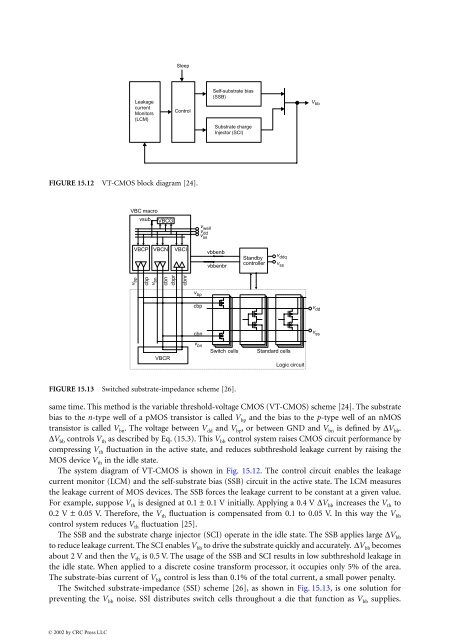
- Page 534 and 535: Masayuki Miyazaki Hitachi, Ltd. 15.
- Page 536 and 537: 15.3 Supply Voltage Management Supp
- Page 538 and 539: FIGURE 15.4 MT-CMOS balloon circuit
- Page 540 and 541: FIGURE 15.9 EVT-CMOS circuit design
- Page 544 and 545: FIGURE 15.15 SA-V t CMOS scheme wit
- Page 546 and 547: FIGURE 15.17 Floating-point datapat
- Page 548 and 549: Vivek De Intel Corporation Ali Kesh
- Page 550 and 551: FIGURE 16.3 n-channel ID vs. VG sho
- Page 552 and 553: Gate-Induced Drain Leakage (I 4) GI
- Page 554 and 555: FIGURE 16.7 Two-nMOS stack in a two
- Page 556 and 557: FIGURE 16.11 Four-input NAND NMOS s
- Page 558 and 559: FIGURE 16.12 Distribution of standb
- Page 560 and 561: Die count FIGURE 16.16 (a) Adaptive
- Page 562 and 563: due to adaptive body bias worsens w
- Page 564 and 565: Thomas D. Burd University of Califo
- Page 566 and 567: the parameter to be maximized since
- Page 568 and 569: 17.3 Dynamically Varying Voltage If
- Page 570 and 571: The voltage converter required for
- Page 572 and 573: FIGURE 17.7 DVS improvement for UI
- Page 574 and 575: FIGURE 17.10 Measured throughput vs
- Page 576 and 577: FIGURE 17.12 Sources of noise margi
- Page 578 and 579: FIGURE 17.15 Ring oscillator adapti
- Page 580 and 581: FIGURE 17.17 Sense-amp delay variat
- Page 582 and 583: Christian Piguet CSEM: Centre Suiss
- Page 584 and 585: Some Basic Rules There are some bas
- Page 586 and 587: TABLE 18.2 Looped 8-bit Multiply Pr
- Page 588 and 589: FIGURE 18.4 new architecture paradi
- Page 590 and 591: FIGURE 18.6 FIGURE 18.7 the second
- Page 592 and 593:
FIGURE 18.9 FIGURE 18.10 With latch
- Page 594 and 595:
18.6 Low-Power Memories As memories
- Page 596 and 597:
connected to the main bitline (only
- Page 598 and 599:
is today only about a factor of 2 d
- Page 600 and 601:
Katsunori Seno SONY Corporation 19.
- Page 602 and 603:
FIGURE 19.2 FIGURE 19.3 This is a c
- Page 604 and 605:
FIGURE 19.6 FIGURE 19.7 FPGA sacrif
- Page 606 and 607:
FIGURE 19.9 RAWn precharge FIGURE 1
- Page 608 and 609:
a fixed given standard. References
- Page 610 and 611:
Hendrawan Soeleman Purdue Universit
- Page 612 and 613:
for a short period of time when bot
- Page 614 and 615:
Total Average Power Putting togethe
- Page 616 and 617:
Signal Probability Calculation In c
- Page 618 and 619:
Example Given y = x 1 + x 2. Find P
- Page 620 and 621:
A B F FIGURE 20.7 Unfactorized and
- Page 622 and 623:
etween successive transitions is a
- Page 624 and 625:
FIGURE 20.9 A logic gate and its co
- Page 626 and 627:
Results Using Probabilistic Techniq
- Page 628 and 629:
FIGURE 20.12 Probabilistic and stat
- Page 630 and 631:
14. VLSI Microprocessors: A Guide t
- Page 632 and 633:
0 V to a voltage V in time T throug
- Page 634 and 635:
a small fraction of circuit nodes t
- Page 636 and 637:
FIGURE 21.6 (a) E-R latch, (b) timi
- Page 638 and 639:
FIGURE 21.8 Potential E-R latch for
- Page 640 and 641:
The only difference between the two
- Page 642 and 643:
FIGURE 21.14 (a) Clock-powered stat
- Page 644 and 645:
FIGURE 21.17 The three drivers used
- Page 646 and 647:
FIGURE 21.20 Energy-delay product (
- Page 648 and 649:
FIGURE 21.22 AC-1 clock-driver sche
- Page 650 and 651:
clock-powered nodes accounted for 8
- Page 652 and 653:
Two generations of clock-powered mi
- Page 654 and 655:
29. Athas, W. C., Tzartzanis, N., M
- Page 656 and 657:
Wayne Wolf Princeton University 22.
- Page 658 and 659:
so a CPU could be built in reconfig
- Page 660 and 661:
optimized processes. Although embed
- Page 662 and 663:
FIGURE 22.4 they are most useful wh
- Page 664 and 665:
• How should processes be allocat
- Page 666 and 667:
25 memory system activity. If the c
- Page 668 and 669:
Jonathan W. Valvano University of T
- Page 670 and 671:
FIGURE 23.2 6808, I/O ports A and B
- Page 672 and 673:
personnel so that they are proficie
- Page 674 and 675:
BDM can provide the ability to obse
- Page 676 and 677:
minor modifications to the finite s
- Page 678 and 679:
Many components are included in a d
- Page 680 and 681:
will saturate resulting in a bang-b
- Page 682 and 683:
Two approaches are used to synchron
- Page 684 and 685:
Fred J. Taylor University of Florid
- Page 686 and 687:
The output of a linear system havin
- Page 688 and 689:
FIGURE 24.2 Effects of windowing an
- Page 690 and 691:
frequency range ±f Nyquist = ±f s
- Page 692 and 693:
performance, complexity, and precis
- Page 694 and 695:
overflows of intermediate sums. Tha
- Page 696 and 697:
24.7 Applications “DSP” has bec
- Page 698 and 699:
DSP (Digital Signal Processor) or D
- Page 700 and 701:
PC as a Terminal (Modem) The PC is
- Page 702 and 703:
characteristics: • Fixed pictures
- Page 704 and 705:
HDTV (and Digital Television) If th
- Page 706 and 707:
Modem Banks This is the first of th
- Page 708 and 709:
25.7 Automotive, Industrial Althoug
- Page 710 and 711:
36. MITEL Semiconductor: www.semico
- Page 712 and 713:
26.2 Digital Filters The theory of
- Page 714 and 715:
|H | 1 FIGURE 26.1 Frequency select
- Page 716 and 717:
TABLE 26.1 Filter Design Comparison
- Page 718 and 719:
frequency response involves some al
- Page 720 and 721:
Impulse Response 0.2 0.15 0.1 0.05
- Page 722 and 723:
This constrained magnitude problem
- Page 724 and 725:
FIGURE 26.8 Block diagram of the ge
- Page 726 and 727:
11. Ikehara, M., Tanaka, H., and Ku
- Page 728 and 729:
Adam Dabrowski Poznan University To
- Page 730 and 731:
−12 2 The reference in this case
- Page 732 and 733:
FIGURE 27.1 Two-band filter bank: (
- Page 734 and 735:
FIGURE 27.5 Critical bandwidth and
- Page 736 and 737:
FIGURE 27.7 Threshold of audibility
- Page 738 and 739:
FIGURE 27.10 Critical band index in
- Page 740 and 741:
FIGURE 27.13 Simplified model of th
- Page 742 and 743:
All described masking effects are e
- Page 744 and 745:
where From Eqs. (27.32) and (27.33)
- Page 746 and 747:
eal-time. Although floating-point p
- Page 748 and 749:
FIGURE 27.19 Overlapped, power comp
- Page 750 and 751:
FIGURE 27.21 Symmetrical FIR filter
- Page 752 and 753:
In the MPEG-1 encoder an efficient
- Page 754 and 755:
These first two approaches can be m
- Page 756 and 757:
FIGURE 27.27 ADPCM: (a) encoder, (b
- Page 758 and 759:
FIGURE 27.30 General scheme of the
- Page 760 and 761:
A new standard MPEG-7, named the mu
- Page 762 and 763:
FIGURE 27.32 AC-3 encoder. FIGURE 2
- Page 764 and 765:
29. Marven, C. and Ewers, G., A sim
- Page 766 and 767:
FIGURE 28.1 FIGURE 28.2 of the huma
- Page 768 and 769:
FIGURE 28.5 image of reasonable qua
- Page 770 and 771:
Consider the case of a simple 2-D
- Page 772 and 773:
FIGURE 28.8 A sampled spatiotempora
- Page 774 and 775:
oth high spatial frequency componen
- Page 776 and 777:
If it were separable (that is, H(ξ
- Page 778 and 779:
The first hypothesis (the less plau
- Page 780 and 781:
FIGURE 28.17 The real (top) and ima
- Page 782 and 783:
FIGURE 28.18 The resolution of a ti
- Page 784 and 785:
FIGURE 28.20 Motion estimation by b
- Page 786 and 787:
where the superscripts n and n + 1
- Page 788 and 789:
must be found via a finite set of o
- Page 790 and 791:
The methods in this subsection are
- Page 792 and 793:
FIGURE 28.28 The split phase. Using
- Page 794 and 795:
35. Y.-T. Wu, T. Kanade, J. Cohn, a
- Page 796 and 797:
29.2 Power Dissipation in Digital C
- Page 798 and 799:
additional power benefits. Efficien
- Page 800 and 801:
Power savings are higher than simpl
- Page 802 and 803:
A priori knowledge of data stream d
- Page 804 and 805:
FIGURE 29.7 DCT Chip [my DCT] avera
- Page 806 and 807:
19. S. Uramoto et al. A 100 MHz 2-D
- Page 808 and 809:
Anna Hać University of Hawaii 30.1
- Page 810 and 811:
Using TCP/IP also makes the network
- Page 812 and 813:
this is for one mobile host which i
- Page 814 and 815:
TDMA Time-division multiple access
- Page 816 and 817:
path delay. The two measures of the
- Page 818 and 819:
are under the control of the system
- Page 820 and 821:
the bandwidth reserved in the targe
- Page 822 and 823:
Chik-Kong Ken Yang University of Ca
- Page 824 and 825:
FIGURE 31.3 attenuation (dB) -3.0 -
- Page 826 and 827:
FIGURE 31.5 to handle large voltage
- Page 828 and 829:
p_o V bias FIGURE 31.8 High-impedan
- Page 830 and 831:
out[n] a0 FIGURE 31.11 Transmitter
- Page 832 and 833:
FIGURE 31.15 Receiver design using
- Page 834 and 835:
digitally by first feeding the inpu
- Page 836 and 837:
FIGURE 31.19 90 o locking using XOR
- Page 838 and 839:
Power of these links is becoming an
- Page 840 and 841:
46. Takahashi, T. et al., “A CMOS
- Page 842 and 843:
Many computer programs exhibit some
- Page 844 and 845:
32.3 Related Memory Models, Hierarc
- Page 846 and 847:
32.6 External Sorting and Related P
- Page 848 and 849:
uns, each striped across the disks.
- Page 850 and 851:
Matrix transposition is the special
- Page 852 and 853:
of satellite images is over one ter
- Page 854 and 855:
TABLE 32.3 Best Known I/O Bounds fo
- Page 856 and 857:
e accessed directly in a single I/O
- Page 858 and 859:
implementations of priority queues
- Page 860 and 861:
By the reduction in [52], a data st
- Page 862 and 863:
set of experiments on various text
- Page 864 and 865:
3. A. Acharya, M. Uysal, and J. Sal
- Page 866 and 867:
44. J. L. Bentley and J. B. Saxe. D
- Page 868 and 869:
85. P. Ferragina and F. Luccio. Dyn
- Page 870 and 871:
128. V. Kumar and E. Schwabe. Impro
- Page 872 and 873:
173. H. Samet. The Design and Analy
- Page 874 and 875:
Peter J. Varman Rice University 33.
- Page 876 and 877:
need for fast transfers, up to 1 Gb
- Page 878 and 879:
In contrast to prefetching that mas
- Page 880 and 881:
The ERF algorithm was analyzed in [
- Page 882 and 883:
increment lowestPriorityOnDisk(disk
- Page 884 and 885:
External or out-of-core algorithms
- Page 886 and 887:
33. M. Kallahalla and P. J. Varman.
- Page 888 and 889:
advanced, reaching the point where
- Page 890 and 891:
FIGURE 34.3 FIGURE 34.4 defines the
- Page 892 and 893:
FIGURE 34.5 Trellis representation
- Page 894 and 895:
FIGURE 34.7 Data and servo sectors.
- Page 896 and 897:
References 1. S. H. Charrap, P. L.
- Page 898 and 899:
High-frequency noise is then remove
- Page 900 and 901:
The various components of (34.3) ar
- Page 902 and 903:
sequences are more complex, and occ
- Page 904 and 905:
ange of 10 −12 -10 −15 . Anothe
- Page 906 and 907:
strategies are reviewed, which have
- Page 908 and 909:
FIGURE 34.13 Magnitude response for
- Page 910 and 911:
taps as an approximation of the Typ
- Page 912 and 913:
FIGURE 34.18 CTF BER performance de
- Page 914 and 915:
TABLE 34.1 Examples of Equalizers I
- Page 916 and 917:
(i) Symbol rate VCO based timing re
- Page 918 and 919:
Symbol Rate Timing Recovery Schemes
- Page 920 and 921:
where B = B 1 + B 2 + 1 is the size
- Page 922 and 923:
in � out � d(k) FIGURE 34.26 Ti
- Page 924 and 925:
�(k) z -L FIGURE 34.27 Linearized
- Page 926 and 927:
10 −4 and 10 −2 . The steady-st
- Page 928 and 929:
16. J. Sonntag, et al., “A high s
- Page 930 and 931:
y a special sequence known as the a
- Page 932 and 933:
FIGURE 34.36 An example of two Gray
- Page 934 and 935:
track n track n +1 FIGURE 34.38 The
- Page 936 and 937:
FIGURE 34.40 The phase format. Posi
- Page 938 and 939:
increase linear density while mitig
- Page 940 and 941:
FIGURE 34.43 Two equivalent constra
- Page 942 and 943:
FIGURE 34.44 Possible pairs of sequ
- Page 944 and 945:
Distance δ min,C can be bounded as
- Page 946 and 947:
FIGURE 34.45 Standard concatenation
- Page 948 and 949:
30. E. Soljanin, “On-track and of
- Page 950 and 951:
The next block is PRE. What is PR?
- Page 952 and 953:
In the above example, we see that s
- Page 954 and 955:
FIGURE 34.52 Feedback detector. Cat
- Page 956 and 957:
FIGURE 34.54 Decision feedback equa
- Page 958 and 959:
esponse (this is also valid for dif
- Page 960 and 961:
its use, while the computational, o
- Page 962 and 963:
FIGURE 34.58 Viterbi algorithm dete
- Page 964 and 965:
Noise-Predictive Maximum Likelihood
- Page 966 and 967:
The error event likelihoods are cal
- Page 968 and 969:
Metric-First Algorithms Metric-firs
- Page 970 and 971:
termination at the same time. Howev
- Page 972 and 973:
13. J. Hagenauer, “Applications o
- Page 974 and 975:
Given a code C of length n and dime
- Page 976 and 977:
Notice that, although a code may ha
- Page 978 and 979:
Not many perfect codes exist. In th
- Page 980 and 981:
Theorem 1 (Shannon) For any � > 0
- Page 982 and 983:
If we write the codewords as polyno
- Page 984 and 985:
Let © 2002 by CRC Press LLC 1 1 K
- Page 986 and 987:
which, in polynomial form, is Let E
- Page 988 and 989:
m Σl=0 because a l = (a m+1 − 1)
- Page 990 and 991:
Evaluating the syndromes, we obtain
- Page 992 and 993:
FIGURE 34.63 Interleaving m times o
- Page 994 and 995:
Operating System © 2002 by CRC Pre
- Page 996 and 997:
systems, the most notable example b
- Page 998 and 999:
35.3 Components of Distributed Oper
- Page 1000 and 1001:
Message-passing IPC shares many cha
- Page 1002 and 1003:
process at any arbitrary stage in i
- Page 1004 and 1005:
Few attempts were made in the past
- Page 1006 and 1007:
alternate years with SOSP), and the
- Page 1008 and 1009:
© 2002 by CRC Press LLC 42 Mobile
- Page 1010 and 1011:
FIGURE 36.1 were introduced; howeve
- Page 1012 and 1013:
FPGAs by providing on-chip memory f
- Page 1014 and 1015:
FIGURE 36.3 There is a considerable
- Page 1016 and 1017:
FIGURE 36.4 The general form of the
- Page 1018 and 1019:
FIGURE 36.6 If a VPB can cover all
- Page 1020 and 1021:
John Morris University of Western A
- Page 1022 and 1023:
FIGURE 37.1 Simplified block diagra
- Page 1024 and 1025:
inverters, and the programmable mul
- Page 1026 and 1027:
Programmable Active Memories (PAM)
- Page 1028 and 1029:
measured in megabits, not megabytes
- Page 1030 and 1031:
from modern FPGAs, e.g., Altera’s
- Page 1032 and 1033:
Regularity A processing pipeline wi
- Page 1034 and 1035:
Other Languages Other routes from h
- Page 1036 and 1037:
29. Bergmann, N.W., and Dawood, A.,
- Page 1038 and 1039:
FIGURE 37.8 Basic architectures for
- Page 1040 and 1041:
Selected Applications Several class
- Page 1042 and 1043:
Development Systems Developing appl
- Page 1044 and 1045:
implementation. Reconfigurable or r
- Page 1046 and 1047:
The designer starts the generation
- Page 1048 and 1049:
lock but allows multiple instructio
- Page 1050 and 1051:
data-types that are mapped to TIE r
- Page 1052 and 1053:
Conclusions Configurable and extens
- Page 1054 and 1055:
FIGURE 38.1 Average vehicle speed.
- Page 1056 and 1057:
AHS means advanced cruise-assist hi
- Page 1058 and 1059:
TABLE 38.3 navigation systems VICS
- Page 1060 and 1061:
FIGURE 38.9 FIGURE 38.10 a map data
- Page 1062 and 1063:
FIGURE 38.13 The four basic functio
- Page 1064 and 1065:
Support of Safe Driving System The
- Page 1066 and 1067:
System evaluation, the fourth issue
- Page 1068 and 1069:
FIGURE 38.18 Summarizing the three
- Page 1070 and 1071:
uilder tools serving to build MMI o
- Page 1072 and 1073:
FIGURE 38.23 FIGURE 38.24 automaker
- Page 1074 and 1075:
FIGURE 38.26 FIGURE 38.27 The first
- Page 1076 and 1077:
FIGURE 38.30 FIGURE 38.31 a kind of
- Page 1078 and 1079:
To Probe Further In this field, the
- Page 1080 and 1081:
FIGURE 39.1 of more versatile media
- Page 1082 and 1083:
1 • 3DNow! 1 [11,12] from AMD,
- Page 1084 and 1085:
FIGURE 39.6 In the packed add instr
- Page 1086 and 1087:
If saturation arithmetic is used in
- Page 1088 and 1089:
TABLE 39.1 Examples of Operations T
- Page 1090 and 1091:
FIGURE 39.10 PAVG R c, R a, R b: Pa
- Page 1092 and 1093:
FIGURE 39.13 Packed compare instruc
- Page 1094 and 1095:
FIGURE 39.17 Packed multiply high i
- Page 1096 and 1097:
FIGURE 39.20 Packed multiply left i
- Page 1098 and 1099:
FIGURE 39.23 In the packed multiply
- Page 1100 and 1101:
TABLE 39.4 Packed Integer Multiplic
- Page 1102 and 1103:
Subword Permutation Instructions In
- Page 1104 and 1105:
is n log 2(n). Table 39.6 shows how
- Page 1106 and 1107:
FIGURE 39.33 Mix left instruction.
- Page 1108 and 1109:
TABLE 39.7 Subword Permutation Inst
- Page 1110 and 1111:
TABLE 39.9 IA-64 uses FPMA and FPMS
- Page 1112 and 1113:
The two-bit result field is written
- Page 1114 and 1115:
source register. These three FP mix
- Page 1116 and 1117:
13. Motorola, “AltiVec technology
- Page 1118 and 1119:
FIGURE 39.48 ManArray 1 × 2 core e
- Page 1120 and 1121:
FIGURE 39.50 Hypercube interconnect
- Page 1122 and 1123:
FIGURE 39.53 Host DSP software laye
- Page 1124 and 1125:
Benchmark Data Type Performance 256
- Page 1126 and 1127:
FIGURE 39.56 Simplified schematic o
- Page 1128 and 1129:
Gaming applications often require a
- Page 1130 and 1131:
system, and the application program
- Page 1132 and 1133:
FIGURE 39.60 FIGURE 39.61 FIGURE 39
- Page 1134 and 1135:
FIGURE 39.64 shifting place limits
- Page 1136 and 1137:
FIGURE 39.66 pitch Address Looping
- Page 1138 and 1139:
FIGURE 39.69 gain of the filter. It
- Page 1140 and 1141:
as a core to integrate onto the sam
- Page 1142 and 1143:
7. Rossum, D., Constraint based aud
- Page 1144 and 1145:
FIGURE 39.74 Procedure for simulate
- Page 1146 and 1147:
The fitness value of an individual
- Page 1148 and 1149:
FIGURE 39.77 The tabu list can be v
- Page 1150 and 1151:
Intermediate-term memory component
- Page 1152 and 1153:
FIGURE 39.81 Selection. FIGURE 39.8
- Page 1154 and 1155:
Work on parallelization of the tabu
- Page 1156 and 1157:
Acknowledgment The authors acknowle
- Page 1158 and 1159:
47. L. K. Grover. A new Simulated A
- Page 1160 and 1161:
93. E. M. Rudnick, J. H. Patel, G.
- Page 1162 and 1163:
138. Youn-Long Lin, Yu-Chin Hsu, an
- Page 1164 and 1165:
This architecture allowed for large
- Page 1166 and 1167:
FIGURE 40.3 40.3 Application Server
- Page 1168 and 1169:
FIGURE 40.5 applications. CORBA cur
- Page 1170 and 1171:
FIGURE 40.8 The application server
- Page 1172 and 1173:
FIGURE 40.10 The proposed architect
- Page 1174 and 1175:
cost at the front end. The ideal ap
- Page 1176 and 1177:
FIGURE 40.12 Client-server and netw
- Page 1178 and 1179:
Yoshiaki Hagiwara Sony Corporation
- Page 1180 and 1181:
FIGURE 41.2 This corresponds to the
- Page 1182 and 1183:
FIGURE 41.5 Buried channel CCD stru
- Page 1184 and 1185:
FIGURE 41.8 Applications of CCD and
- Page 1186 and 1187:
sensor (1100 K pixel) Microphone ×
- Page 1188 and 1189:
�� �� FIGURE 41.14 Form com
- Page 1190 and 1191:
FIGURE 41.16 Stack technology. Link
- Page 1192 and 1193:
1st EmDRAM Product FIGURE 41.19 Emb
- Page 1194 and 1195:
FIGURE 41.23 Em-DRAM process techno
- Page 1196 and 1197:
John F. Alexander University of Nor
- Page 1198 and 1199:
Several reasons exist for mentionin
- Page 1200 and 1201:
sort of local area network. Support
- Page 1202 and 1203:
Technological hurdles must be overc
- Page 1204 and 1205:
FIGURE 42.1 Block diagram of (a) ge
- Page 1206 and 1207:
FIGURE 42.3 Alternative FIR filter
- Page 1208 and 1209:
FIGURE 42.5 Polyphase filter struct
- Page 1210 and 1211:
3. E. Dahlman, Bjorn Gudmundson, M.
- Page 1212 and 1213:
TABLE 42.1 Categorizing Reusable Co
- Page 1214 and 1215:
FIGURE 42.11 Internet growth. FIGUR
- Page 1216 and 1217:
FIGURE 42.13 Software for VoIP SoC.
- Page 1218 and 1219:
FIGURE 42.17 Bandwidth trends. FIGU
- Page 1220 and 1221:
The interconnections between the va
- Page 1222 and 1223:
FIGURE 42.21 A typical communicatio
- Page 1224 and 1225:
carry information over longer dista
- Page 1226 and 1227:
however, it is not uncommon that so
- Page 1228 and 1229:
node, to which the user is connecte
- Page 1230 and 1231:
its information. Intuitively, this
- Page 1232 and 1233:
This issue is referred to as latenc
- Page 1234 and 1235:
Evolution of Standard Image/Video C
- Page 1236 and 1237:
FIGURE 42.26 Sequence of zigzag-cod
- Page 1238 and 1239:
FIGURE 42.29 150th Frame of origina
- Page 1240 and 1241:
FIGURE 42.31 Data partitioning for
- Page 1242 and 1243:
for transmitting a predictively cod
- Page 1244 and 1245:
42.6 Pen-Based User Interfaces—An
- Page 1246 and 1247:
FIGURE 42.35 The handwriting recogn
- Page 1248 and 1249:
• No toggling between edit/contro
- Page 1250 and 1251:
FIGURE 42.39 Boxplots of time to en
- Page 1252 and 1253:
0 … 9 ( ) -
- Page 1254 and 1255:
is using the SMIL generic media ref
- Page 1256 and 1257:
FIGURE 42.47 Example of pen-and-pap
- Page 1258 and 1259:
slots specifying pieces of informat
- Page 1260 and 1261:
most stringent demands for low-powe
- Page 1262 and 1263:
FIGURE 42.51 MIPS requirement of se
- Page 1264 and 1265:
FIGURE 42.54 von Neumann architectu
- Page 1266 and 1267:
FIGURE 42.57 Dual Mac architecture
- Page 1268 and 1269:
FIGURE 42.59 Two data path variatio
- Page 1270 and 1271:
FIGURE 42.60 Basic pipeline archite
- Page 1272 and 1273:
References 1. Bahl L., Cocke J., Je
- Page 1274 and 1275:
Random Oracle Model One direction o
- Page 1276 and 1277:
at the end of its usefulness. A new
- Page 1278 and 1279:
function and verification function
- Page 1280 and 1281:
underlies the Diffie-Hellman key ag
- Page 1282 and 1283:
31. Dolev, D., Dwork, C., and Naor,
- Page 1284 and 1285:
R. Chandramouli Synopsys Inc. 44.1
- Page 1286 and 1287:
many deficiencies in the design may
- Page 1288 and 1289:
impact the performance and test ove
- Page 1290 and 1291:
FIGURE 44.4 FIGURE 44.5 It becomes
- Page 1292 and 1293:
SoC methodologies require synchroni
- Page 1294 and 1295:
This method, however, lacks the app
- Page 1296 and 1297:
FIGURE 45.2 Input formats of MILEF
- Page 1298 and 1299:
FIGURE 45.3 FIGURE 45.4 Robustness
- Page 1300 and 1301:
FIGURE 45.5 In Fig. 45.5 a simple e
- Page 1302 and 1303:
difficult to identify for overcurre
- Page 1304 and 1305:
General Approach in Comparison with
- Page 1306 and 1307:
FIGURE 45.10 phase—the propagatio
- Page 1308 and 1309:
shorter test sequence could possibl
- Page 1310 and 1311:
Looking at results of Table 45.6, i
- Page 1312 and 1313:
45.4 Summary Automatic test pattern
- Page 1314 and 1315:
41. F. Brglez, H. Fujiwara: A neutr
- Page 1316 and 1317:
FIGURE 46.1 Rule of ten in testing
- Page 1318 and 1319:
FIGURE 46.5 FIGURE 46.6 of the DUT.
- Page 1320 and 1321:
FIGURE 46.7 generate tests for ever
- Page 1322 and 1323:
FIGURE 46.9 FIGURE 46.10 behavioral
- Page 1324 and 1325:
Z. Stamenković University of N. St
- Page 1326 and 1327:
FIGURE 47.2 Murphy’s Model The mo
- Page 1328 and 1329:
where k is the total number of crit
- Page 1330 and 1331:
FIGURE 47.5 Definition of IC critic
- Page 1332 and 1333:
distribution [34,35]: © 2002 by CR
- Page 1334 and 1335:
and, in the case of w = X 2 − X 1
- Page 1336 and 1337:
Algorithm • Input: a singly linke
- Page 1338 and 1339:
TRACIF takes a CIF file as input an
- Page 1340 and 1341:
TABLE 47.2 Critical Area Extraction
- Page 1342 and 1343:
Also, the critical areas for lithog
- Page 1344 and 1345:
(enhancement of the process cleanli
- Page 1346 and 1347:
28. Corsi, F. and Martino, S., Defe