Attention! Your ePaper is waiting for publication!
By publishing your document, the content will be optimally indexed by Google via AI and sorted into the right category for over 500 million ePaper readers on YUMPU.
This will ensure high visibility and many readers!

Your ePaper is now published and live on YUMPU!
You can find your publication here:
Share your interactive ePaper on all platforms and on your website with our embed function


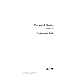
ARM Architecture Reference Manual ARMv7-A and ARMv7-R edition
ARM Architecture Reference Manual ARMv7-A and ARMv7-R edition
ARM Architecture Reference Manual ARMv7-A and ARMv7-R edition

Create successful ePaper yourself
Turn your PDF publications into a flip-book with our unique Google optimized e-Paper software.
Debug Registers <strong>Reference</strong><br />
Table C10-18 Interaction of CP15 Cache Behavior Override Register (CBOR) <strong>and</strong> DBGDSCCR<br />
DBGDSCCR setting CBOR setting Debug state Behavior<br />
nWT = 1 WT = 0 X Areas marked WB are Write-Back<br />
nWT = X WT = 0 No Areas marked WB are Write-Back<br />
nWT = X WT = 1 X Areas marked WB are Write-Through<br />
nWT = 0 WT = X Yes Areas marked WB are Write-Through<br />
nDL = 1 DL = 0 X Data or unified cache linefills are enabled<br />
nDL = X DL = 0 No Data or unified cache linefills are enabled<br />
nDL = X DL = 1 X Data or unified cache linefills are disabled<br />
nDL = 0 DL = X Yes Data or unified cache linefills are disabled<br />
nIL = 1 IL = 0 X Instruction cache linefills are enabled<br />
nIL = X IL = 0 No Instruction cache linefills are enabled<br />
nIL = X IL = 1 X Instruction cache linefills are disabled<br />
nIL = 0 IL = X Yes Instruction cache linefills are disabled<br />
A processor that does not implement Security Extensions has only WT, IL <strong>and</strong> DL settings in the CP15<br />
Cache Behavior Override Register. Processors that implement Security Extensions can have separate<br />
settings for, for example, NS_WT <strong>and</strong> S_WT in the CP15 Cache Behavior Override Register. For brevity<br />
Table C10-18 does not show the full matrix of possibilities in this case. For the behavior on such a processor,<br />
duplicate Table C10-18:<br />
once for the Non-secure case, for example NS_WT<br />
once for the Secure case, for example S_WT.<br />
C10.7.2 Debug State MMU Control Register (DBGDSMCR)<br />
The Debug State MMU Control Register, DBGDSMCR, controls TLB behavior when the processor is in<br />
Debug state.<br />
The DBGDSMCR is:<br />
debug register 11, at offset 0x02C<br />
a read/write register, with some bits that might not be implemented <strong>and</strong> therefore are RAZ/WI<br />
required in v7 Debug<br />
when the Security Extensions are implemented, a Common register.<br />
C10-84 Copyright © 1996-1998, 2000, 2004-2008 <strong>ARM</strong> Limited. All rights reserved. <strong>ARM</strong> DDI 0406B

Debug Registers <strong>Reference</strong> Table C10-18 Interaction of CP15 Cache Behavior Override Register (CBOR) <strong>and</strong> DBGDSCCR DBGDSCCR setting CBOR setting Debug state Behavior nWT = 1 WT = 0 X Areas marked WB are Write-Back nWT = X WT = 0 No Areas marked WB are Write-Back nWT = X WT = 1 X Areas marked WB are Write-Through nWT = 0 WT = X Yes Areas marked WB are Write-Through nDL = 1 DL = 0 X Data or unified cache linefills are enabled nDL = X DL = 0 No Data or unified cache linefills are enabled nDL = X DL = 1 X Data or unified cache linefills are disabled nDL = 0 DL = X Yes Data or unified cache linefills are disabled nIL = 1 IL = 0 X Instruction cache linefills are enabled nIL = X IL = 0 No Instruction cache linefills are enabled nIL = X IL = 1 X Instruction cache linefills are disabled nIL = 0 IL = X Yes Instruction cache linefills are disabled A processor that does not implement Security Extensions has only WT, IL <strong>and</strong> DL settings in the CP15 Cache Behavior Override Register. Processors that implement Security Extensions can have separate settings for, for example, NS_WT <strong>and</strong> S_WT in the CP15 Cache Behavior Override Register. For brevity Table C10-18 does not show the full matrix of possibilities in this case. For the behavior on such a processor, duplicate Table C10-18: once for the Non-secure case, for example NS_WT once for the Secure case, for example S_WT. C10.7.2 Debug State MMU Control Register (DBGDSMCR) The Debug State MMU Control Register, DBGDSMCR, controls TLB behavior when the processor is in Debug state. The DBGDSMCR is: debug register 11, at offset 0x02C a read/write register, with some bits that might not be implemented <strong>and</strong> therefore are RAZ/WI required in v7 Debug when the Security Extensions are implemented, a Common register. C10-84 Copyright © 1996-1998, 2000, 2004-2008 <strong>ARM</strong> Limited. All rights reserved. <strong>ARM</strong> DDI 0406B
Debug Registers <strong>Reference</strong> It is IMPLEMENTATION DEFINED whether the DBGDSMCR is included in a v6 Debug or v6.1 Debug implementation. The format of the DBGDSMCR is: 31 4 Reserved, UNK/SBZP Bits [31:4] Reserved, UNK/SBZP. TLB matching bits, bits [3:2] Instruction TLB matching, nIUM Data TLB matching, nDUM Instruction TLB loading, nIUL Data TLB loading, nDUL Either or both of these bits might not be implemented, in which case the bit is RAZ/WI. If implemented these bits are: nIUM, bit [3] Instruction TLB matching bit, where separate Data <strong>and</strong> Instruction TLBs are implemented. nDUM, bit [2] Data or Unified TLB matching bit. The possible values of an implemented TLB matching bit are: 0 Request disabling of TLB matching for memory operations issued by a debugger when the processor is in Debug state 1 Normal operation of TLB matching for memory operations issued by a debugger when the processor is in Debug state. When TLB matching is disabled, all memory accesses normally checked against a TLB are not checked against the TLB. For every access the next level of translation is performed. The results are not cached in the TLB, <strong>and</strong> no TLB entries are evicted. The next level of translation is used for every access. The next level of translation might mean looking in the next level TLB, or doing a translation table walk, depending on the numbers of levels of TLB implemented. Note If TLB matching is disabled, <strong>and</strong> TLB maintenance functions have not been correctly performed by the system being debugged, for example, if the TLB has not been flushed following a change to the translation tables, memory accesses made by the debugger might not undergo the same virtual to physical memory mappings as the application being debugged. A debugger can create temporary alternative memory mappings by altering the contents of the external translation tables <strong>and</strong> disabling all levels of TLB matching. However, for normal debugging operations, <strong>ARM</strong> recommends that the TLB Matching bit is set to 1. <strong>ARM</strong> DDI 0406B Copyright © 1996-1998, 2000, 2004-2008 <strong>ARM</strong> Limited. All rights reserved. C10-85 3 2 1 0
- Page 1 and 2:
® ARM Architecture Reference Manua
- Page 3 and 4:
This ARM Architecture Reference Man
- Page 5 and 6:
Contents ARM Architecture Reference
- Page 7 and 8:
Contents Chapter A6 Thumb Instructi
- Page 9 and 10:
Contents C1.3 Security Extensions a
- Page 11 and 12:
Contents Appendix D Deprecated and
- Page 13 and 14:
Preface This preface summarizes the
- Page 15 and 16:
Using this manual The information i
- Page 17 and 18:
Part D, Appendices This manual cont
- Page 19 and 20:
Assembler syntax descriptions This
- Page 21 and 22:
Feedback ARM welcomes feedback on i
- Page 23:
Part A Application Level Architectu
- Page 26 and 27:
Introduction to the ARM Architectur
- Page 28 and 29:
Introduction to the ARM Architectur
- Page 30 and 31:
Introduction to the ARM Architectur
- Page 32 and 33:
Introduction to the ARM Architectur
- Page 34 and 35:
Application Level Programmers’ Mo
- Page 36 and 37:
Application Level Programmers’ Mo
- Page 38 and 39:
Application Level Programmers’ Mo
- Page 40 and 41:
Application Level Programmers’ Mo
- Page 42 and 43:
Application Level Programmers’ Mo
- Page 44 and 45:
Application Level Programmers’ Mo
- Page 46 and 47:
Application Level Programmers’ Mo
- Page 48 and 49:
Application Level Programmers’ Mo
- Page 50 and 51:
Application Level Programmers’ Mo
- Page 52 and 53:
Application Level Programmers’ Mo
- Page 54 and 55:
Application Level Programmers’ Mo
- Page 56 and 57:
Application Level Programmers’ Mo
- Page 58 and 59:
Application Level Programmers’ Mo
- Page 60 and 61:
Application Level Programmers’ Mo
- Page 62 and 63:
Application Level Programmers’ Mo
- Page 64 and 65:
Application Level Programmers’ Mo
- Page 66 and 67:
Application Level Programmers’ Mo
- Page 68 and 69:
Application Level Programmers’ Mo
- Page 70 and 71:
Application Level Programmers’ Mo
- Page 72 and 73:
Application Level Programmers’ Mo
- Page 74 and 75:
Application Level Programmers’ Mo
- Page 76 and 77:
Application Level Programmers’ Mo
- Page 78 and 79:
Application Level Programmers’ Mo
- Page 80 and 81:
Application Level Programmers’ Mo
- Page 82 and 83:
Application Level Programmers’ Mo
- Page 84 and 85:
Application Level Programmers’ Mo
- Page 86 and 87:
Application Level Programmers’ Mo
- Page 88 and 89:
Application Level Programmers’ Mo
- Page 90 and 91:
Application Level Programmers’ Mo
- Page 92 and 93:
Application Level Programmers’ Mo
- Page 94 and 95:
Application Level Programmers’ Mo
- Page 96 and 97:
Application Level Programmers’ Mo
- Page 98 and 99:
Application Level Programmers’ Mo
- Page 100 and 101:
Application Level Programmers’ Mo
- Page 102 and 103:
Application Level Programmers’ Mo
- Page 104 and 105:
Application Level Programmers’ Mo
- Page 106 and 107:
Application Level Programmers’ Mo
- Page 108 and 109:
Application Level Programmers’ Mo
- Page 110 and 111:
Application Level Programmers’ Mo
- Page 112 and 113:
Application Level Programmers’ Mo
- Page 114 and 115:
Application Level Programmers’ Mo
- Page 116 and 117:
Application Level Memory Model A3.1
- Page 118 and 119:
Application Level Memory Model A3.2
- Page 120 and 121:
Application Level Memory Model A3.2
- Page 122 and 123:
Application Level Memory Model The
- Page 124 and 125:
Application Level Memory Model Reve
- Page 126 and 127:
Application Level Memory Model A3.4
- Page 128 and 129:
Application Level Memory Model When
- Page 130 and 131:
Application Level Memory Model A3.4
- Page 132 and 133:
Application Level Memory Model Open
- Page 134 and 135:
Application Level Memory Model Excl
- Page 136 and 137:
Application Level Memory Model If t
- Page 138 and 139:
Application Level Memory Model A3.5
- Page 140 and 141:
Application Level Memory Model Memo
- Page 142 and 143:
Application Level Memory Model If a
- Page 144 and 145:
Application Level Memory Model Non-
- Page 146 and 147:
Application Level Memory Model Writ
- Page 148 and 149:
Application Level Memory Model All
- Page 150 and 151:
Application Level Memory Model To e
- Page 152 and 153:
Application Level Memory Model A3.6
- Page 154 and 155:
Application Level Memory Model A3.7
- Page 156 and 157:
Application Level Memory Model A3.8
- Page 158 and 159:
Application Level Memory Model a re
- Page 160 and 161:
Application Level Memory Model A1 I
- Page 162 and 163:
Application Level Memory Model The
- Page 164 and 165:
Application Level Memory Model In a
- Page 166 and 167:
Application Level Memory Model A3.9
- Page 168 and 169:
Application Level Memory Model A3.9
- Page 170 and 171:
The Instruction Sets A4.1 About the
- Page 172 and 173:
The Instruction Sets A4.2 Unified A
- Page 174 and 175:
The Instruction Sets This alternati
- Page 176 and 177:
The Instruction Sets A4.4 Data-proc
- Page 178 and 179:
The Instruction Sets Instruction Mn
- Page 180 and 181:
The Instruction Sets Signed Most Si
- Page 182 and 183:
The Instruction Sets A4.4.5 Packing
- Page 184 and 185:
The Instruction Sets A4.4.7 Paralle
- Page 186 and 187:
The Instruction Sets A4.5 Status re
- Page 188 and 189:
The Instruction Sets A4.6.3 Unprivi
- Page 190 and 191:
The Instruction Sets A4.7 Load/stor
- Page 192 and 193:
The Instruction Sets A4.9 Exception
- Page 194 and 195:
The Instruction Sets A4.11 Advanced
- Page 196 and 197:
The Instruction Sets Table A4-14 El
- Page 198 and 199:
The Instruction Sets A4.13 Advanced
- Page 200 and 201:
The Instruction Sets Table A4-16 Ad
- Page 202 and 203:
The Instruction Sets A4.13.4 Advanc
- Page 204 and 205:
The Instruction Sets A4.13.6 Miscel
- Page 206 and 207:
The Instruction Sets A4.14 VFP data
- Page 208 and 209:
ARM Instruction Set Encoding A5.1 A
- Page 210 and 211:
ARM Instruction Set Encoding A5.2 D
- Page 212 and 213:
ARM Instruction Set Encoding Table
- Page 214 and 215:
ARM Instruction Set Encoding A5.2.3
- Page 216 and 217:
ARM Instruction Set Encoding Carry
- Page 218 and 219:
ARM Instruction Set Encoding A5.2.5
- Page 220 and 221:
ARM Instruction Set Encoding A5.2.8
- Page 222 and 223:
ARM Instruction Set Encoding A5.2.1
- Page 224 and 225:
ARM Instruction Set Encoding A5.2.1
- Page 226 and 227:
ARM Instruction Set Encoding 1 xx1x
- Page 228 and 229:
ARM Instruction Set Encoding A5.4.1
- Page 230 and 231:
ARM Instruction Set Encoding A5.4.3
- Page 232 and 233:
ARM Instruction Set Encoding A5.4.4
- Page 234 and 235:
ARM Instruction Set Encoding A5.6 S
- Page 236 and 237:
ARM Instruction Set Encoding A5.7 U
- Page 238 and 239:
ARM Instruction Set Encoding 110x00
- Page 240 and 241:
Thumb Instruction Set Encoding A6.1
- Page 242 and 243:
Thumb Instruction Set Encoding If t
- Page 244 and 245:
Thumb Instruction Set Encoding A6.2
- Page 246 and 247:
Thumb Instruction Set Encoding A6.2
- Page 248 and 249:
Thumb Instruction Set Encoding A6.2
- Page 250 and 251:
Thumb Instruction Set Encoding If-T
- Page 252 and 253:
Thumb Instruction Set Encoding A6.3
- Page 254 and 255:
Thumb Instruction Set Encoding Tabl
- Page 256 and 257:
Thumb Instruction Set Encoding Carr
- Page 258 and 259:
Thumb Instruction Set Encoding A6.3
- Page 260 and 261:
Thumb Instruction Set Encoding 0100
- Page 262 and 263:
Thumb Instruction Set Encoding A6.3
- Page 264 and 265:
Thumb Instruction Set Encoding A6.3
- Page 266 and 267:
Thumb Instruction Set Encoding A6.3
- Page 268 and 269:
Thumb Instruction Set Encoding A6.3
- Page 270 and 271:
Thumb Instruction Set Encoding Tabl
- Page 272 and 273:
Thumb Instruction Set Encoding op1
- Page 274 and 275:
Thumb Instruction Set Encoding A6.3
- Page 276 and 277:
Thumb Instruction Set Encoding A6.3
- Page 278 and 279:
Thumb Instruction Set Encoding A6.3
- Page 280 and 281:
Thumb Instruction Set Encoding A6-4
- Page 282 and 283:
Advanced SIMD and VFP Instruction E
- Page 284 and 285:
Advanced SIMD and VFP Instruction E
- Page 286 and 287:
Advanced SIMD and VFP Instruction E
- Page 288 and 289:
Advanced SIMD and VFP Instruction E
- Page 290 and 291:
Advanced SIMD and VFP Instruction E
- Page 292 and 293:
Advanced SIMD and VFP Instruction E
- Page 294 and 295:
Advanced SIMD and VFP Instruction E
- Page 296 and 297:
Advanced SIMD and VFP Instruction E
- Page 298 and 299:
Advanced SIMD and VFP Instruction E
- Page 300 and 301:
Advanced SIMD and VFP Instruction E
- Page 302 and 303:
Advanced SIMD and VFP Instruction E
- Page 304 and 305:
Advanced SIMD and VFP Instruction E
- Page 306 and 307:
Advanced SIMD and VFP Instruction E
- Page 308 and 309:
Advanced SIMD and VFP Instruction E
- Page 310 and 311:
Advanced SIMD and VFP Instruction E
- Page 312 and 313:
Advanced SIMD and VFP Instruction E
- Page 314 and 315:
Instruction Details A8.1 Format of
- Page 316 and 317:
Instruction Details A8.1.4 Assemble
- Page 318 and 319:
Instruction Details A8.1.6 Exceptio
- Page 320 and 321:
Instruction Details A8.3 Conditiona
- Page 322 and 323:
Instruction Details A8.4 Shifts app
- Page 324 and 325:
Instruction Details if imm5 == ‘0
- Page 326 and 327:
Instruction Details A8.6 Alphabetic
- Page 328 and 329:
Instruction Details A8.6.2 ADC (reg
- Page 330 and 331:
Instruction Details A8.6.3 ADC (reg
- Page 332 and 333:
Instruction Details A8.6.4 ADD (imm
- Page 334 and 335:
Instruction Details A8.6.5 ADD (imm
- Page 336 and 337:
Instruction Details A8.6.6 ADD (reg
- Page 338 and 339:
Instruction Details A8.6.7 ADD (reg
- Page 340 and 341:
Instruction Details A8.6.8 ADD (SP
- Page 342 and 343:
Instruction Details A8.6.9 ADD (SP
- Page 344 and 345:
Instruction Details A8.6.10 ADR Thi
- Page 346 and 347:
Instruction Details A8.6.11 AND (im
- Page 348 and 349:
Instruction Details A8.6.12 AND (re
- Page 350 and 351:
Instruction Details A8.6.13 AND (re
- Page 352 and 353:
Instruction Details A8.6.14 ASR (im
- Page 354 and 355:
Instruction Details A8.6.15 ASR (re
- Page 356 and 357:
Instruction Details A8.6.16 B Branc
- Page 358 and 359:
Instruction Details A8.6.17 BFC Bit
- Page 360 and 361:
Instruction Details A8.6.18 BFI Bit
- Page 362 and 363:
Instruction Details A8.6.19 BIC (im
- Page 364 and 365:
Instruction Details A8.6.20 BIC (re
- Page 366 and 367:
Instruction Details A8.6.21 BIC (re
- Page 368 and 369:
Instruction Details A8.6.22 BKPT Br
- Page 370 and 371:
Instruction Details A8.6.23 BL, BLX
- Page 372 and 373:
Instruction Details A8.6.24 BLX (re
- Page 374 and 375:
Instruction Details A8.6.25 BX Bran
- Page 376 and 377:
Instruction Details A8.6.26 BXJ Bra
- Page 378 and 379:
Instruction Details A8.6.27 CBNZ, C
- Page 380 and 381:
Instruction Details A8.6.28 CDP, CD
- Page 382 and 383:
Instruction Details A8.6.29 CHKA A8
- Page 384 and 385:
Instruction Details A8.6.31 CLZ Cou
- Page 386 and 387:
Instruction Details A8.6.32 CMN (im
- Page 388 and 389:
Instruction Details A8.6.33 CMN (re
- Page 390 and 391:
Instruction Details A8.6.34 CMN (re
- Page 392 and 393:
Instruction Details A8.6.35 CMP (im
- Page 394 and 395:
Instruction Details A8.6.36 CMP (re
- Page 396 and 397:
Instruction Details A8.6.37 CMP (re
- Page 398 and 399:
Instruction Details A8.6.38 CPS A8.
- Page 400 and 401:
Instruction Details A8.6.40 DBG Deb
- Page 402 and 403:
Instruction Details A8.6.41 DMB Dat
- Page 404 and 405:
Instruction Details A8.6.42 DSB Dat
- Page 406 and 407:
Instruction Details A8.6.43 ENTERX
- Page 408 and 409:
Instruction Details A8.6.45 EOR (re
- Page 410 and 411:
Instruction Details A8.6.46 EOR (re
- Page 412 and 413:
Instruction Details A8.6.47 F* (for
- Page 414 and 415:
Instruction Details A8.6.48 HB, HBL
- Page 416 and 417:
Instruction Details A8.6.50 IT If T
- Page 418 and 419:
Instruction Details A8.6.51 LDC, LD
- Page 420 and 421:
Instruction Details A8.6.52 LDC, LD
- Page 422 and 423:
Instruction Details A8.6.53 LDM / L
- Page 424 and 425:
Instruction Details A8.6.54 LDMDA /
- Page 426 and 427:
Instruction Details A8.6.55 LDMDB /
- Page 428 and 429:
Instruction Details A8.6.56 LDMIB /
- Page 430 and 431:
Instruction Details A8.6.57 LDR (im
- Page 432 and 433:
Instruction Details A8.6.58 LDR (im
- Page 434 and 435:
Instruction Details A8.6.59 LDR (li
- Page 436 and 437:
Instruction Details A8.6.60 LDR (re
- Page 438 and 439:
Instruction Details A8.6.61 LDRB (i
- Page 440 and 441:
Instruction Details A8.6.62 LDRB (i
- Page 442 and 443:
Instruction Details A8.6.63 LDRB (l
- Page 444 and 445:
Instruction Details A8.6.64 LDRB (r
- Page 446 and 447:
Instruction Details A8.6.65 LDRBT L
- Page 448 and 449:
Instruction Details A8.6.66 LDRD (i
- Page 450 and 451:
Instruction Details A8.6.67 LDRD (l
- Page 452 and 453:
Instruction Details A8.6.68 LDRD (r
- Page 454 and 455:
Instruction Details A8.6.69 LDREX L
- Page 456 and 457:
Instruction Details A8.6.70 LDREXB
- Page 458 and 459:
Instruction Details A8.6.71 LDREXD
- Page 460 and 461:
Instruction Details A8.6.72 LDREXH
- Page 462 and 463:
Instruction Details A8.6.73 LDRH (i
- Page 464 and 465:
Instruction Details A8.6.74 LDRH (i
- Page 466 and 467:
Instruction Details A8.6.75 LDRH (l
- Page 468 and 469:
Instruction Details A8.6.76 LDRH (r
- Page 470 and 471:
Instruction Details A8.6.77 LDRHT L
- Page 472 and 473:
Instruction Details A8.6.78 LDRSB (
- Page 474 and 475:
Instruction Details A8.6.79 LDRSB (
- Page 476 and 477:
Instruction Details A8.6.80 LDRSB (
- Page 478 and 479:
Instruction Details A8.6.81 LDRSBT
- Page 480 and 481:
Instruction Details A8.6.82 LDRSH (
- Page 482 and 483:
Instruction Details A8.6.83 LDRSH (
- Page 484 and 485:
Instruction Details A8.6.84 LDRSH (
- Page 486 and 487:
Instruction Details A8.6.85 LDRSHT
- Page 488 and 489:
Instruction Details A8.6.86 LDRT Lo
- Page 490 and 491:
Instruction Details A8.6.87 LEAVEX
- Page 492 and 493:
Instruction Details A8.6.89 LSL (re
- Page 494 and 495:
Instruction Details A8.6.90 LSR (im
- Page 496 and 497:
Instruction Details A8.6.91 LSR (re
- Page 498 and 499:
Instruction Details A8.6.92 MCR, MC
- Page 500 and 501:
Instruction Details A8.6.93 MCRR, M
- Page 502 and 503:
Instruction Details A8.6.94 MLA Mul
- Page 504 and 505:
Instruction Details A8.6.95 MLS Mul
- Page 506 and 507:
Instruction Details A8.6.96 MOV (im
- Page 508 and 509:
Instruction Details A8.6.97 MOV (re
- Page 510 and 511:
Instruction Details A8.6.98 MOV (sh
- Page 512 and 513:
Instruction Details A8.6.99 MOVT Mo
- Page 514 and 515:
Instruction Details A8.6.100 MRC, M
- Page 516 and 517:
Instruction Details A8.6.101 MRRC,
- Page 518 and 519:
Instruction Details A8.6.102 MRS Mo
- Page 520 and 521:
Instruction Details A8.6.103 MSR (i
- Page 522 and 523:
Instruction Details A8.6.104 MSR (r
- Page 524 and 525:
Instruction Details A8.6.105 MUL Mu
- Page 526 and 527:
Instruction Details A8.6.106 MVN (i
- Page 528 and 529:
Instruction Details A8.6.107 MVN (r
- Page 530 and 531:
Instruction Details A8.6.108 MVN (r
- Page 532 and 533:
Instruction Details A8.6.109 NEG Ne
- Page 534 and 535:
Instruction Details A8.6.110 NOP No
- Page 536 and 537:
Instruction Details A8.6.111 ORN (i
- Page 538 and 539:
Instruction Details A8.6.112 ORN (r
- Page 540 and 541:
Instruction Details A8.6.113 ORR (i
- Page 542 and 543:
Instruction Details A8.6.114 ORR (r
- Page 544 and 545:
Instruction Details A8.6.115 ORR (r
- Page 546 and 547:
Instruction Details A8.6.116 PKH Pa
- Page 548 and 549:
Instruction Details A8.6.117 PLD, P
- Page 550 and 551:
Instruction Details A8.6.118 PLD (l
- Page 552 and 553:
Instruction Details A8.6.119 PLD, P
- Page 554 and 555:
Instruction Details A8.6.120 PLI (i
- Page 556 and 557:
Instruction Details A8.6.121 PLI (r
- Page 558 and 559:
Instruction Details A8.6.122 POP Po
- Page 560 and 561:
Instruction Details A8.6.123 PUSH P
- Page 562 and 563:
Instruction Details A8.6.124 QADD S
- Page 564 and 565:
Instruction Details A8.6.125 QADD16
- Page 566 and 567:
Instruction Details A8.6.126 QADD8
- Page 568 and 569:
Instruction Details A8.6.127 QASX S
- Page 570 and 571:
Instruction Details A8.6.128 QDADD
- Page 572 and 573:
Instruction Details A8.6.129 QDSUB
- Page 574 and 575:
Instruction Details A8.6.130 QSAX S
- Page 576 and 577:
Instruction Details A8.6.131 QSUB S
- Page 578 and 579:
Instruction Details A8.6.132 QSUB16
- Page 580 and 581:
Instruction Details A8.6.133 QSUB8
- Page 582 and 583:
Instruction Details A8.6.134 RBIT R
- Page 584 and 585:
Instruction Details A8.6.135 REV By
- Page 586 and 587:
Instruction Details A8.6.136 REV16
- Page 588 and 589:
Instruction Details A8.6.137 REVSH
- Page 590 and 591:
Instruction Details A8.6.138 RFE Re
- Page 592 and 593:
Instruction Details A8.6.140 ROR (r
- Page 594 and 595:
Instruction Details A8.6.141 RRX Ro
- Page 596 and 597:
Instruction Details A8.6.142 RSB (i
- Page 598 and 599:
Instruction Details A8.6.143 RSB (r
- Page 600 and 601:
Instruction Details A8.6.144 RSB (r
- Page 602 and 603:
Instruction Details A8.6.145 RSC (i
- Page 604 and 605:
Instruction Details A8.6.146 RSC (r
- Page 606 and 607:
Instruction Details A8.6.147 RSC (r
- Page 608 and 609:
Instruction Details A8.6.148 SADD16
- Page 610 and 611:
Instruction Details A8.6.149 SADD8
- Page 612 and 613:
Instruction Details A8.6.150 SASX S
- Page 614 and 615:
Instruction Details A8.6.151 SBC (i
- Page 616 and 617:
Instruction Details A8.6.152 SBC (r
- Page 618 and 619:
Instruction Details A8.6.153 SBC (r
- Page 620 and 621:
Instruction Details A8.6.154 SBFX S
- Page 622 and 623:
Instruction Details A8.6.155 SDIV S
- Page 624 and 625:
Instruction Details A8.6.156 SEL Se
- Page 626 and 627:
Instruction Details A8.6.157 SETEND
- Page 628 and 629:
Instruction Details A8.6.158 SEV Se
- Page 630 and 631:
Instruction Details A8.6.159 SHADD1
- Page 632 and 633:
Instruction Details A8.6.160 SHADD8
- Page 634 and 635:
Instruction Details A8.6.161 SHASX
- Page 636 and 637:
Instruction Details A8.6.162 SHSAX
- Page 638 and 639:
Instruction Details A8.6.163 SHSUB1
- Page 640 and 641:
Instruction Details A8.6.164 SHSUB8
- Page 642 and 643:
Instruction Details A8.6.165 SMC (p
- Page 644 and 645:
Instruction Details A8.6.167 SMLAD
- Page 646 and 647:
Instruction Details A8.6.168 SMLAL
- Page 648 and 649:
Instruction Details A8.6.169 SMLALB
- Page 650 and 651:
Instruction Details A8.6.170 SMLALD
- Page 652 and 653:
Instruction Details A8.6.171 SMLAWB
- Page 654 and 655:
Instruction Details A8.6.172 SMLSD
- Page 656 and 657:
Instruction Details A8.6.173 SMLSLD
- Page 658 and 659:
Instruction Details A8.6.174 SMMLA
- Page 660 and 661:
Instruction Details A8.6.175 SMMLS
- Page 662 and 663:
Instruction Details A8.6.176 SMMUL
- Page 664 and 665:
Instruction Details A8.6.177 SMUAD
- Page 666 and 667:
Instruction Details A8.6.178 SMULBB
- Page 668 and 669:
Instruction Details A8.6.179 SMULL
- Page 670 and 671:
Instruction Details A8.6.180 SMULWB
- Page 672 and 673:
Instruction Details A8.6.181 SMUSD
- Page 674 and 675:
Instruction Details A8.6.182 SRS A8
- Page 676 and 677:
Instruction Details A8.6.184 SSAT16
- Page 678 and 679:
Instruction Details A8.6.185 SSAX S
- Page 680 and 681:
Instruction Details A8.6.186 SSUB16
- Page 682 and 683:
Instruction Details A8.6.187 SSUB8
- Page 684 and 685:
Instruction Details A8.6.188 STC, S
- Page 686 and 687:
Instruction Details A8.6.189 STM /
- Page 688 and 689:
Instruction Details A8.6.190 STMDA
- Page 690 and 691:
Instruction Details A8.6.191 STMDB
- Page 692 and 693:
Instruction Details A8.6.192 STMIB
- Page 694 and 695:
Instruction Details A8.6.193 STR (i
- Page 696 and 697:
Instruction Details A8.6.194 STR (i
- Page 698 and 699:
Instruction Details A8.6.195 STR (r
- Page 700 and 701:
Instruction Details A8.6.196 STRB (
- Page 702 and 703:
Instruction Details A8.6.197 STRB (
- Page 704 and 705:
Instruction Details A8.6.198 STRB (
- Page 706 and 707:
Instruction Details A8.6.199 STRBT
- Page 708 and 709:
Instruction Details A8.6.200 STRD (
- Page 710 and 711:
Instruction Details A8.6.201 STRD (
- Page 712 and 713:
Instruction Details A8.6.202 STREX
- Page 714 and 715:
Instruction Details A8.6.203 STREXB
- Page 716 and 717:
Instruction Details A8.6.204 STREXD
- Page 718 and 719:
Instruction Details A8.6.205 STREXH
- Page 720 and 721:
Instruction Details A8.6.206 STRH (
- Page 722 and 723:
Instruction Details A8.6.207 STRH (
- Page 724 and 725:
Instruction Details A8.6.208 STRH (
- Page 726 and 727:
Instruction Details A8.6.209 STRHT
- Page 728 and 729:
Instruction Details A8.6.210 STRT S
- Page 730 and 731:
Instruction Details A8.6.211 SUB (i
- Page 732 and 733:
Instruction Details A8.6.212 SUB (i
- Page 734 and 735:
Instruction Details A8.6.213 SUB (r
- Page 736 and 737:
Instruction Details A8.6.214 SUB (r
- Page 738 and 739:
Instruction Details A8.6.215 SUB (S
- Page 740 and 741:
Instruction Details A8.6.216 SUB (S
- Page 742 and 743:
Instruction Details A8.6.217 SUBS P
- Page 744 and 745:
Instruction Details A8.6.219 SWP, S
- Page 746 and 747:
Instruction Details A8.6.220 SXTAB
- Page 748 and 749:
Instruction Details A8.6.221 SXTAB1
- Page 750 and 751:
Instruction Details A8.6.222 SXTAH
- Page 752 and 753:
Instruction Details A8.6.223 SXTB S
- Page 754 and 755:
Instruction Details A8.6.224 SXTB16
- Page 756 and 757:
Instruction Details A8.6.225 SXTH S
- Page 758 and 759:
Instruction Details A8.6.226 TBB, T
- Page 760 and 761:
Instruction Details A8.6.227 TEQ (i
- Page 762 and 763:
Instruction Details A8.6.228 TEQ (r
- Page 764 and 765:
Instruction Details A8.6.229 TEQ (r
- Page 766 and 767:
Instruction Details A8.6.230 TST (i
- Page 768 and 769:
Instruction Details A8.6.231 TST (r
- Page 770 and 771:
Instruction Details A8.6.232 TST (r
- Page 772 and 773:
Instruction Details A8.6.233 UADD16
- Page 774 and 775:
Instruction Details A8.6.234 UADD8
- Page 776 and 777:
Instruction Details A8.6.235 UASX U
- Page 778 and 779:
Instruction Details A8.6.236 UBFX U
- Page 780 and 781:
Instruction Details A8.6.237 UDIV U
- Page 782 and 783:
Instruction Details A8.6.238 UHADD1
- Page 784 and 785:
Instruction Details A8.6.239 UHADD8
- Page 786 and 787:
Instruction Details A8.6.240 UHASX
- Page 788 and 789:
Instruction Details A8.6.241 UHSAX
- Page 790 and 791:
Instruction Details A8.6.242 UHSUB1
- Page 792 and 793:
Instruction Details A8.6.243 UHSUB8
- Page 794 and 795:
Instruction Details A8.6.244 UMAAL
- Page 796 and 797:
Instruction Details A8.6.245 UMLAL
- Page 798 and 799:
Instruction Details A8.6.246 UMULL
- Page 800 and 801:
Instruction Details A8.6.247 UQADD1
- Page 802 and 803:
Instruction Details A8.6.248 UQADD8
- Page 804 and 805:
Instruction Details A8.6.249 UQASX
- Page 806 and 807:
Instruction Details A8.6.250 UQSAX
- Page 808 and 809:
Instruction Details A8.6.251 UQSUB1
- Page 810 and 811:
Instruction Details A8.6.252 UQSUB8
- Page 812 and 813:
Instruction Details A8.6.253 USAD8
- Page 814 and 815:
Instruction Details A8.6.254 USADA8
- Page 816 and 817:
Instruction Details A8.6.255 USAT U
- Page 818 and 819:
Instruction Details A8.6.256 USAT16
- Page 820 and 821:
Instruction Details A8.6.257 USAX U
- Page 822 and 823:
Instruction Details A8.6.258 USUB16
- Page 824 and 825:
Instruction Details A8.6.259 USUB8
- Page 826 and 827:
Instruction Details A8.6.260 UXTAB
- Page 828 and 829:
Instruction Details A8.6.261 UXTAB1
- Page 830 and 831:
Instruction Details A8.6.262 UXTAH
- Page 832 and 833:
Instruction Details A8.6.263 UXTB U
- Page 834 and 835:
Instruction Details A8.6.264 UXTB16
- Page 836 and 837:
Instruction Details A8.6.265 UXTH U
- Page 838 and 839:
Instruction Details A8.6.266 VABA,
- Page 840 and 841:
Instruction Details A8.6.267 VABD,
- Page 842 and 843:
Instruction Details A8.6.268 VABD (
- Page 844 and 845:
Instruction Details A8.6.269 VABS V
- Page 846 and 847:
Instruction Details A8.6.270 VACGE,
- Page 848 and 849:
Instruction Details A8.6.271 VADD (
- Page 850 and 851:
Instruction Details A8.6.272 VADD (
- Page 852 and 853:
Instruction Details A8.6.273 VADDHN
- Page 854 and 855:
Instruction Details A8.6.274 VADDL,
- Page 856 and 857:
Instruction Details A8.6.275 VAND (
- Page 858 and 859:
Instruction Details A8.6.277 VBIC (
- Page 860 and 861:
Instruction Details A8.6.278 VBIC (
- Page 862 and 863:
Instruction Details A8.6.279 VBIF,
- Page 864 and 865:
Instruction Details A8.6.280 VCEQ (
- Page 866 and 867:
Instruction Details A8.6.281 VCEQ (
- Page 868 and 869:
Instruction Details A8.6.282 VCGE (
- Page 870 and 871:
Instruction Details A8.6.283 VCGE (
- Page 872 and 873:
Instruction Details A8.6.284 VCGT (
- Page 874 and 875:
Instruction Details A8.6.285 VCGT (
- Page 876 and 877:
Instruction Details A8.6.286 VCLE (
- Page 878 and 879:
Instruction Details A8.6.288 VCLS V
- Page 880 and 881:
Instruction Details A8.6.289 VCLT (
- Page 882 and 883:
Instruction Details A8.6.291 VCLZ V
- Page 884 and 885:
Instruction Details A8.6.292 VCMP,
- Page 886 and 887:
Instruction Details A8.6.293 VCNT T
- Page 888 and 889:
Instruction Details A8.6.294 VCVT (
- Page 890 and 891:
Instruction Details A8.6.295 VCVT,
- Page 892 and 893:
Instruction Details A8.6.296 VCVT (
- Page 894 and 895:
Instruction Details A8.6.297 VCVT (
- Page 896 and 897:
Instruction Details A8.6.298 VCVT (
- Page 898 and 899:
Instruction Details A8.6.299 VCVT (
- Page 900 and 901:
Instruction Details A8.6.300 VCVTB,
- Page 902 and 903:
Instruction Details A8.6.301 VDIV T
- Page 904 and 905:
Instruction Details A8.6.302 VDUP (
- Page 906 and 907:
Instruction Details A8.6.303 VDUP (
- Page 908 and 909:
Instruction Details A8.6.304 VEOR V
- Page 910 and 911:
Instruction Details A8.6.305 VEXT V
- Page 912 and 913:
Instruction Details A8.6.306 VHADD,
- Page 914 and 915:
Instruction Details A8.6.307 VLD1 (
- Page 916 and 917:
Instruction Details A8.6.308 VLD1 (
- Page 918 and 919:
Instruction Details A8.6.309 VLD1 (
- Page 920 and 921:
Instruction Details A8.6.310 VLD2 (
- Page 922 and 923:
Instruction Details A8.6.311 VLD2 (
- Page 924 and 925:
Instruction Details A8.6.312 VLD2 (
- Page 926 and 927:
Instruction Details A8.6.313 VLD3 (
- Page 928 and 929:
Instruction Details A8.6.314 VLD3 (
- Page 930 and 931:
Instruction Details A8.6.315 VLD3 (
- Page 932 and 933:
Instruction Details A8.6.316 VLD4 (
- Page 934 and 935:
Instruction Details A8.6.317 VLD4 (
- Page 936 and 937:
Instruction Details A8.6.318 VLD4 (
- Page 938 and 939:
Instruction Details A8.6.319 VLDM V
- Page 940 and 941:
Instruction Details A8.6.320 VLDR T
- Page 942 and 943:
Instruction Details A8.6.321 VMAX,
- Page 944 and 945:
Instruction Details A8.6.322 VMAX,
- Page 946 and 947:
Instruction Details A8.6.323 VMLA,
- Page 948 and 949:
Instruction Details A8.6.324 VMLA,
- Page 950 and 951:
Instruction Details A8.6.325 VMLA,
- Page 952 and 953:
Instruction Details A8.6.326 VMOV (
- Page 954 and 955:
Instruction Details A8.6.327 VMOV (
- Page 956 and 957:
Instruction Details A8.6.328 VMOV (
- Page 958 and 959:
Instruction Details A8.6.329 VMOV (
- Page 960 and 961:
Instruction Details A8.6.330 VMOV (
- Page 962 and 963:
Instruction Details A8.6.331 VMOV (
- Page 964 and 965:
Instruction Details A8.6.332 VMOV (
- Page 966 and 967:
Instruction Details A8.6.333 VMOVL
- Page 968 and 969:
Instruction Details A8.6.334 VMOVN
- Page 970 and 971:
Instruction Details A8.6.335 VMRS M
- Page 972 and 973:
Instruction Details A8.6.336 VMSR M
- Page 974 and 975:
Instruction Details A8.6.337 VMUL,
- Page 976 and 977:
Instruction Details A8.6.338 VMUL (
- Page 978 and 979:
Instruction Details A8.6.339 VMUL,
- Page 980 and 981:
Instruction Details A8.6.340 VMVN (
- Page 982 and 983:
Instruction Details A8.6.341 VMVN (
- Page 984 and 985:
Instruction Details A8.6.342 VNEG V
- Page 986 and 987:
Instruction Details A8.6.343 VNMLA,
- Page 988 and 989:
Instruction Details A8.6.344 VORN (
- Page 990 and 991:
Instruction Details A8.6.346 VORR (
- Page 992 and 993:
Instruction Details A8.6.347 VORR (
- Page 994 and 995:
Instruction Details A8.6.348 VPADAL
- Page 996 and 997:
Instruction Details A8.6.349 VPADD
- Page 998 and 999:
Instruction Details A8.6.350 VPADD
- Page 1000 and 1001:
Instruction Details A8.6.351 VPADDL
- Page 1002 and 1003:
Instruction Details A8.6.352 VPMAX,
- Page 1004 and 1005:
Instruction Details A8.6.353 VPMAX,
- Page 1006 and 1007:
Instruction Details A8.6.354 VPOP V
- Page 1008 and 1009:
Instruction Details A8.6.355 VPUSH
- Page 1010 and 1011:
Instruction Details A8.6.356 VQABS
- Page 1012 and 1013:
Instruction Details A8.6.357 VQADD
- Page 1014 and 1015:
Instruction Details A8.6.358 VQDMLA
- Page 1016 and 1017:
Instruction Details A8.6.359 VQDMUL
- Page 1018 and 1019:
Instruction Details A8.6.360 VQDMUL
- Page 1020 and 1021:
Instruction Details A8.6.361 VQMOVN
- Page 1022 and 1023:
Instruction Details A8.6.362 VQNEG
- Page 1024 and 1025:
Instruction Details A8.6.363 VQRDMU
- Page 1026 and 1027:
Instruction Details A8.6.364 VQRSHL
- Page 1028 and 1029:
Instruction Details A8.6.365 VQRSHR
- Page 1030 and 1031:
Instruction Details A8.6.366 VQSHL
- Page 1032 and 1033:
Instruction Details A8.6.367 VQSHL,
- Page 1034 and 1035:
Instruction Details A8.6.368 VQSHRN
- Page 1036 and 1037:
Instruction Details A8.6.369 VQSUB
- Page 1038 and 1039:
Instruction Details A8.6.370 VRADDH
- Page 1040 and 1041:
Instruction Details A8.6.371 VRECPE
- Page 1042 and 1043:
Instruction Details A8.6.372 VRECPS
- Page 1044 and 1045:
Instruction Details A8.6.373 VREV16
- Page 1046 and 1047:
Instruction Details A8.6.374 VRHADD
- Page 1048 and 1049:
Instruction Details A8.6.375 VRSHL
- Page 1050 and 1051:
Instruction Details A8.6.376 VRSHR
- Page 1052 and 1053:
Instruction Details A8.6.377 VRSHRN
- Page 1054 and 1055:
Instruction Details A8.6.378 VRSQRT
- Page 1056 and 1057:
Instruction Details A8.6.379 VRSQRT
- Page 1058 and 1059:
Instruction Details A8.6.380 VRSRA
- Page 1060 and 1061:
Instruction Details A8.6.381 VRSUBH
- Page 1062 and 1063:
Instruction Details A8.6.382 VSHL (
- Page 1064 and 1065:
Instruction Details A8.6.383 VSHL (
- Page 1066 and 1067:
Instruction Details A8.6.384 VSHLL
- Page 1068 and 1069:
Instruction Details A8.6.385 VSHR V
- Page 1070 and 1071:
Instruction Details A8.6.386 VSHRN
- Page 1072 and 1073:
Instruction Details A8.6.387 VSLI V
- Page 1074 and 1075:
Instruction Details A8.6.388 VSQRT
- Page 1076 and 1077:
Instruction Details A8.6.389 VSRA V
- Page 1078 and 1079:
Instruction Details A8.6.390 VSRI V
- Page 1080 and 1081:
Instruction Details A8.6.391 VST1 (
- Page 1082 and 1083:
Instruction Details A8.6.392 VST1 (
- Page 1084 and 1085:
Instruction Details A8.6.393 VST2 (
- Page 1086 and 1087:
Instruction Details A8.6.394 VST2 (
- Page 1088 and 1089:
Instruction Details A8.6.395 VST3 (
- Page 1090 and 1091:
Instruction Details A8.6.396 VST3 (
- Page 1092 and 1093:
Instruction Details A8.6.397 VST4 (
- Page 1094 and 1095:
Instruction Details A8.6.398 VST4 (
- Page 1096 and 1097:
Instruction Details A8.6.399 VSTM V
- Page 1098 and 1099:
Instruction Details A8.6.400 VSTR T
- Page 1100 and 1101:
Instruction Details A8.6.401 VSUB (
- Page 1102 and 1103:
Instruction Details A8.6.402 VSUB (
- Page 1104 and 1105:
Instruction Details A8.6.403 VSUBHN
- Page 1106 and 1107:
Instruction Details A8.6.404 VSUBL,
- Page 1108 and 1109:
Instruction Details A8.6.405 VSWP V
- Page 1110 and 1111:
Instruction Details A8.6.406 VTBL,
- Page 1112 and 1113:
Instruction Details A8.6.407 VTRN D
- Page 1114 and 1115:
Instruction Details A8.6.408 VTST V
- Page 1116 and 1117:
Instruction Details A8.6.409 VUZP V
- Page 1118 and 1119:
Instruction Details A8.6.410 VZIP V
- Page 1120 and 1121:
Instruction Details A8.6.411 WFE Wa
- Page 1122 and 1123:
Instruction Details A8.6.412 WFI Wa
- Page 1124 and 1125:
Instruction Details A8.6.413 YIELD
- Page 1126 and 1127:
Instruction Details A8-814 Copyrigh
- Page 1128 and 1129:
ThumbEE A9.1 The ThumbEE instructio
- Page 1130 and 1131:
ThumbEE A9.1.3 Instructions with mo
- Page 1132 and 1133:
ThumbEE A9.2 ThumbEE instruction se
- Page 1134 and 1135:
ThumbEE A9.4 ThumbEE instructions w
- Page 1136 and 1137:
ThumbEE A9.4.2 LDRH (register) Load
- Page 1138 and 1139:
ThumbEE A9.4.4 STR (register) Store
- Page 1140 and 1141:
ThumbEE A9.5 Additional ThumbEE ins
- Page 1142 and 1143:
ThumbEE A9.5.2 HB, HBL Handler Bran
- Page 1144 and 1145:
ThumbEE A9.5.4 HBP HBP (Handler Bra
- Page 1146 and 1147:
ThumbEE Assembler syntax LDR , [{,
- Page 1148 and 1149:
ThumbEE A9-22 Copyright © 1996-199
- Page 1151 and 1152:
Chapter B1 The System Level Program
- Page 1153 and 1154:
B1.2 System level concepts and term
- Page 1155 and 1156:
An exception is described as synchr
- Page 1157 and 1158:
Notes on the ARM processor modes Th
- Page 1159 and 1160:
B1.3.2 ARM core registers The Syste
- Page 1161 and 1162:
Writing to the PC In ARMv7, instruc
- Page 1163 and 1164:
LookUpRName() // ============= The
- Page 1165 and 1166:
interrupt and asynchronous abort di
- Page 1167 and 1168:
Mask bits, bits [8:6] The System Le
- Page 1169 and 1170:
The System Level Programmers’ Mod
- Page 1171 and 1172:
SPSR[] = bits(32) value if BadMode(
- Page 1173 and 1174:
B1.4 Instruction set states The Sys
- Page 1175 and 1176:
B1.5 The Security Extensions The Sy
- Page 1177 and 1178:
Note It is important to distinguish
- Page 1179 and 1180:
The System Level Programmers’ Mod
- Page 1181 and 1182:
Exception offset Exception that is
- Page 1183 and 1184:
Operation The System Level Programm
- Page 1185 and 1186:
Exception Base LR value a Instructi
- Page 1187 and 1188:
Exception The System Level Programm
- Page 1189 and 1190:
The System Level Programmers’ Mod
- Page 1191 and 1192:
B1.6.5 Exception-handling instructi
- Page 1193 and 1194:
SCR bits FW FIQ Effect on FIQ handl
- Page 1195 and 1196:
The System Level Programmers’ Mod
- Page 1197 and 1198:
The System Level Programmers’ Mod
- Page 1199 and 1200:
The System Level Programmers’ Mod
- Page 1201 and 1202:
The System Level Programmers’ Mod
- Page 1203 and 1204:
B1.6.13 Secure Monitor Call (SMC) e
- Page 1205 and 1206:
new_spsr_value = CPSR; The System L
- Page 1207 and 1208:
CPSR.J = ‘0’; CPSR.T = SCTLR.TE
- Page 1209 and 1210:
The System Level Programmers’ Mod
- Page 1211 and 1212:
The System Level Programmers’ Mod
- Page 1213 and 1214:
The System Level Programmers’ Mod
- Page 1215 and 1216:
The System Level Programmers’ Mod
- Page 1217 and 1218:
Note The System Level Programmers
- Page 1219 and 1220:
The System Level Programmers’ Mod
- Page 1221 and 1222:
In addition: The System Level Progr
- Page 1223 and 1224:
B1.9 Execution environment support
- Page 1225 and 1226:
The System Level Programmers’ Mod
- Page 1227 and 1228:
Jazelle state configuration and con
- Page 1229 and 1230:
Controlling entry to Jazelle state
- Page 1231 and 1232:
Trivial implementation of the Jazel
- Page 1233 and 1234:
The System Level Programmers’ Mod
- Page 1235 and 1236:
Chapter B2 Common Memory System Arc
- Page 1237 and 1238:
B2.2 Caches Common Memory System Ar
- Page 1239 and 1240:
B2.2.2 Cache behavior Common Memory
- Page 1241 and 1242:
Common Memory System Architecture F
- Page 1243 and 1244:
Note Common Memory System Architect
- Page 1245 and 1246:
Common Memory System Architecture F
- Page 1247 and 1248:
Common Memory System Architecture F
- Page 1249 and 1250:
Common Memory System Architecture F
- Page 1251 and 1252:
Common Memory System Architecture F
- Page 1253 and 1254:
implement one of the other permitte
- Page 1255 and 1256:
Common Memory System Architecture F
- Page 1257 and 1258:
Common Memory System Architecture F
- Page 1259 and 1260:
Note Common Memory System Architect
- Page 1261 and 1262:
B2.3 IMPLEMENTATION DEFINED memory
- Page 1263 and 1264:
Common Memory System Architecture F
- Page 1265 and 1266:
when MemArch_PMSA AlignmentFaultP(a
- Page 1267 and 1268:
Note Common Memory System Architect
- Page 1269 and 1270:
B2.4.7 Exclusive monitors operation
- Page 1271 and 1272:
B2.4.8 Access permission checking C
- Page 1273 and 1274:
B2.4.10 Data Abort exception Common
- Page 1275 and 1276:
Chapter B3 Virtual Memory System Ar
- Page 1277 and 1278:
Virtual Memory System Architecture
- Page 1279 and 1280:
B3.2.3 Enabling and disabling the M
- Page 1281 and 1282:
B3.3 Translation tables Virtual Mem
- Page 1283 and 1284:
The other fields in the descriptors
- Page 1285 and 1286:
Additional requirements for transla
- Page 1287 and 1288:
B3.3.3 Translation table walks Virt
- Page 1289 and 1290:
Virtual Memory System Architecture
- Page 1291 and 1292:
Translation flow for a Section Virt
- Page 1293 and 1294:
Translation flow for a Small page V
- Page 1295 and 1296:
B3.3.4 Changing translation table a
- Page 1297 and 1298:
B3.4 Address mapping restrictions V
- Page 1299 and 1300:
Note Virtual Memory System Architec
- Page 1301 and 1302:
B3.5.1 The effect of the Security E
- Page 1303 and 1304:
AP[2] AP[1:0] Virtual Memory System
- Page 1305 and 1306:
B3.6.3 Domains Virtual Memory Syste
- Page 1307 and 1308:
Virtual Memory System Architecture
- Page 1309 and 1310:
Virtual Memory System Architecture
- Page 1311 and 1312:
Virtual Memory System Architecture
- Page 1313 and 1314:
B3.7.4 The effect of the Security E
- Page 1315 and 1316:
Section domain fault Section permis
- Page 1317 and 1318:
Translation fault There are two typ
- Page 1319 and 1320:
B3.8.2 External aborts Virtual Memo
- Page 1321 and 1322:
Virtual Memory System Architecture
- Page 1323 and 1324:
Virtual Memory System Architecture
- Page 1325 and 1326:
DFSR [10,3:0] a Virtual Memory Syst
- Page 1327 and 1328:
B3.9.8 Auxiliary Fault Status Regis
- Page 1329 and 1330:
B3.10.2 TLB matching Virtual Memory
- Page 1331 and 1332:
In the TLB operations: Virtual Memo
- Page 1333 and 1334:
Virtual Memory System Architecture
- Page 1335 and 1336:
Note Virtual Memory System Architec
- Page 1337 and 1338:
Virtual Memory System Architecture
- Page 1339 and 1340:
Virtual Memory System Architecture
- Page 1341 and 1342:
Register and description c1, Secure
- Page 1343 and 1344:
Virtual Memory System Architecture
- Page 1345 and 1346:
Virtual Memory System Architecture
- Page 1347 and 1348:
CP15 register Virtual Memory System
- Page 1349 and 1350:
CP15 register Virtual Memory System
- Page 1351 and 1352:
Virtual Memory System Architecture
- Page 1353 and 1354:
B3.12.6 CP15 c0, ID codes registers
- Page 1355 and 1356:
B3.12.7 c0, Main ID Register (MIDR)
- Page 1357 and 1358:
Accessing the MIDR Virtual Memory S
- Page 1359 and 1360:
B3.12.9 c0, TCM Type Register (TCMT
- Page 1361 and 1362:
B3.12.11 c0, Multiprocessor Affinit
- Page 1363 and 1364:
Virtual Memory System Architecture
- Page 1365 and 1366:
B3.12.12 c0, Cache Size ID Register
- Page 1367 and 1368:
CtypeX, bits [3(x - 1) + 2:3(x - 1)
- Page 1369 and 1370:
B3.12.15 c0, Cache Size Selection R
- Page 1371 and 1372:
When the Security Extensions are im
- Page 1373 and 1374:
Bit [23] RAO/SBOP. Virtual Memory S
- Page 1375 and 1376:
Virtual Memory System Architecture
- Page 1377 and 1378:
Accessing the SCTLR Virtual Memory
- Page 1379 and 1380:
Virtual Memory System Architecture
- Page 1381 and 1382:
nET, bit [6] Not Early Termination.
- Page 1383 and 1384:
The format of the SDER is: 31 Bits
- Page 1385 and 1386:
NSASEDIS, bit[15] Disable Non-secur
- Page 1387 and 1388:
B3.12.23 CP15 c2 and c3, Memory pro
- Page 1389 and 1390:
Virtual Memory System Architecture
- Page 1391 and 1392:
C, bit [0], ARMv7-A base architectu
- Page 1393 and 1394:
Accessing the TTBCR Virtual Memory
- Page 1395 and 1396:
B3.12.28 CP15 c5, Fault status regi
- Page 1397 and 1398:
Virtual Memory System Architecture
- Page 1399 and 1400:
Accessing the DFAR Virtual Memory S
- Page 1401 and 1402:
Virtual Memory System Architecture
- Page 1403 and 1404:
Set/way Virtual Memory System Archi
- Page 1405 and 1406:
Virtual Memory System Architecture
- Page 1407 and 1408:
Note Virtual Memory System Architec
- Page 1409 and 1410:
Virtual Memory System Architecture
- Page 1411 and 1412:
CP15 c7, Data and Instruction Barri
- Page 1413 and 1414:
The CP15 c8 TLB maintenance functio
- Page 1415 and 1416:
Invalidate TLB entries by MVA all A
- Page 1417 and 1418:
The IMPLEMENTATION DEFINED TLB cont
- Page 1419 and 1420:
Virtual Memory System Architecture
- Page 1421 and 1422:
10 Region is WriteThrough, Non-Writ
- Page 1423 and 1424:
Virtual Memory System Architecture
- Page 1425 and 1426:
Virtual Memory System Architecture
- Page 1427 and 1428:
Virtual Memory System Architecture
- Page 1429 and 1430:
Accessing the Software Thread ID re
- Page 1431 and 1432:
B3.13.3 Address translation Virtual
- Page 1433 and 1434:
Virtual Memory System Architecture
- Page 1435 and 1436:
domain = bits(4) UNKNOWN; sectionno
- Page 1437 and 1438:
Chapter B4 Protected Memory System
- Page 1439 and 1440:
All addresses are physical addresse
- Page 1441 and 1442:
Using the default memory map as a b
- Page 1443 and 1444:
Address range Behavior of an implem
- Page 1445 and 1446:
B4.2 Memory access control Protecte
- Page 1447 and 1448:
B4.3 Memory region attributes Prote
- Page 1449 and 1450:
B4.4 PMSA memory aborts Protected M
- Page 1451 and 1452:
The MPU fault checking sequence Fig
- Page 1453 and 1454:
Parity error reporting Protected Me
- Page 1455 and 1456:
B4.5.2 Data Abort exceptions Protec
- Page 1457 and 1458:
Reserved encodings in the IFSR and
- Page 1459 and 1460:
Protected Memory System Architectur
- Page 1461 and 1462:
Protected Memory System Architectur
- Page 1463 and 1464:
Unallocated CP15 encodings Protecte
- Page 1465 and 1466:
B4.6.4 Meaning of fixed bit values
- Page 1467 and 1468:
Protected Memory System Architectur
- Page 1469 and 1470:
Architecture, bits [19:16] Table B4
- Page 1471 and 1472:
DminLine, bits [19:16] Bit [15] RAO
- Page 1473 and 1474:
Protected Memory System Architectur
- Page 1475 and 1476:
Protected Memory System Architectur
- Page 1477 and 1478:
LineSize, bits [2:0] (Log2(Number o
- Page 1479 and 1480:
B4.6.13 c0, IMPLEMENTATION DEFINED
- Page 1481 and 1482:
B4.6.16 c1, System Control Register
- Page 1483 and 1484:
Bit [20] RAZ/SBZP. Protected Memory
- Page 1485 and 1486:
Protected Memory System Architectur
- Page 1487 and 1488:
Accessing the ACTLR Protected Memor
- Page 1489 and 1490:
Protected Memory System Architectur
- Page 1491 and 1492:
Protected Memory System Architectur
- Page 1493 and 1494:
The formats of the ADFSR and AIFSR
- Page 1495 and 1496:
B4.6.24 CP15 c6, Memory region prog
- Page 1497 and 1498:
The DRBAR is: a 32-bit read/write r
- Page 1499 and 1500:
RSize, bits [5:1] Protected Memory
- Page 1501 and 1502:
Protected Memory System Architectur
- Page 1503 and 1504:
Protected Memory System Architectur
- Page 1505 and 1506:
Protected Memory System Architectur
- Page 1507 and 1508:
Set/way Protected Memory System Arc
- Page 1509 and 1510:
Instruction Synchronization Barrier
- Page 1511 and 1512:
B4.6.31 CP15 c11, Reserved for TCM
- Page 1513 and 1514:
B4.6.35 CP15 c13 Software Thread ID
- Page 1515 and 1516:
Protected Memory System Architectur
- Page 1517 and 1518:
B4.7.3 Default memory map attribute
- Page 1519 and 1520:
Chapter B5 The CPUID Identification
- Page 1521 and 1522:
B5.1.2 General features of the CPUI
- Page 1523 and 1524:
State1, bits [7:4] The CPUID Identi
- Page 1525 and 1526:
Memory-mapped trace model, bits [19
- Page 1527 and 1528:
B5.2.4 CP15 c0, Memory Model Featur
- Page 1529 and 1530:
c0, Memory Model Feature Register 1
- Page 1531 and 1532:
The CPUID Identification Scheme 0b0
- Page 1533 and 1534:
Unified TLB, bits [19:16] The CPUID
- Page 1535 and 1536:
c0, Memory Model Feature Register 3
- Page 1537 and 1538:
Accessing the Memory Model Feature
- Page 1539 and 1540:
Multiply instructions The CPUID Ide
- Page 1541 and 1542:
The CPUID Identification Scheme Tab
- Page 1543 and 1544:
Swap_instrs, bits [3:0] The CPUID I
- Page 1545 and 1546:
Endian_instrs, bits [3:0] The CPUID
- Page 1547 and 1548:
c0, Instruction Set Attribute Regis
- Page 1549 and 1550:
Note The CPUID Identification Schem
- Page 1551 and 1552:
Unpriv_instrs, bits [3:0] The CPUID
- Page 1553 and 1554:
The CPUID Identification Scheme SW,
- Page 1555 and 1556:
Square root, bits [23:20] Divide, b
- Page 1557 and 1558:
VFP HPFP, bits[27:24] The CPUID Ide
- Page 1559 and 1560:
Chapter B6 System Instructions This
- Page 1561 and 1562:
B6.1.1 CPS System Instructions Chan
- Page 1563 and 1564:
B6.1.2 LDM (exception return) Syste
- Page 1565 and 1566:
B6.1.3 LDM (user registers) System
- Page 1567 and 1568:
B6.1.4 LDRBT, LDRHT, LDRSBT, LDRSHT
- Page 1569 and 1570:
Assembler syntax MRS , where: See
- Page 1571 and 1572:
Operation if ConditionPassed() then
- Page 1573 and 1574:
Is a sequence of one or more of the
- Page 1575 and 1576:
Assembler syntax RFE{} {!} where:
- Page 1577 and 1578:
Assembler syntax SMC # where: See
- Page 1579 and 1580:
Assembler syntax SRS{} SP{!}, # whe
- Page 1581 and 1582:
Operation if ConditionPassed() then
- Page 1583 and 1584:
B6.1.13 SUBS PC, LR and related ins
- Page 1585 and 1586:
B6.1.14 VMRS System Instructions Mo
- Page 1587 and 1588:
B6.1.15 VMSR System Instructions Mo
- Page 1589:
Part C Debug Architecture
- Page 1592 and 1593:
Introduction to the ARM Debug Archi
- Page 1594 and 1595:
Introduction to the ARM Debug Archi
- Page 1596 and 1597:
Introduction to the ARM Debug Archi
- Page 1598 and 1599:
Introduction to the ARM Debug Archi
- Page 1600 and 1601:
Introduction to the ARM Debug Archi
- Page 1602 and 1603:
Invasive Debug Authentication C2.1
- Page 1604 and 1605:
Invasive Debug Authentication If DB
- Page 1606 and 1607:
Debug Events C3.1 About debug event
- Page 1608 and 1609:
Debug Events BKPT Instruction Break
- Page 1610 and 1611:
Debug Events The following sections
- Page 1612 and 1613:
Debug Events Note For IVA compariso
- Page 1614 and 1615:
Debug Events Note There is no encod
- Page 1616 and 1617:
Debug Events Note v6 Debug does not
- Page 1618 and 1619:
Debug Events Interaction of IVA mis
- Page 1620 and 1621:
Debug Events Watchpoint Value Regis
- Page 1622 and 1623:
Debug Events For the ordering of de
- Page 1624 and 1625:
Debug Events Note To understand why
- Page 1626 and 1627:
Debug Events Note Normally, excepti
- Page 1628 and 1629:
Debug Events Note The FCSE is optio
- Page 1630 and 1631:
Debug Events If these guidelines ar
- Page 1632 and 1633:
Debug Events BreakpointDebugEvent()
- Page 1634 and 1635:
Debug Events when InstrSet_ARM byte
- Page 1636 and 1637:
Debug Events if DBGBCR[M] != ‘11
- Page 1638 and 1639:
Debug Events else if IsSecure() the
- Page 1640 and 1641:
Debug Events // WRPMatch() // =====
- Page 1642 and 1643:
Debug Events C3.3 Halting debug eve
- Page 1644 and 1645:
Debug Events C3.4 Generation of deb
- Page 1646 and 1647:
Debug Events As a result, for an in
- Page 1648 and 1649:
Debug Events Debug events must be t
- Page 1650 and 1651:
Debug Exceptions C4.1 About debug e
- Page 1652 and 1653:
Debug Exceptions C4.2 Effects of de
- Page 1654 and 1655:
Debug Exceptions C4-6 Copyright ©
- Page 1656 and 1657:
Debug State C5.1 About Debug state
- Page 1658 and 1659:
Debug State 3. The processor signal
- Page 1660 and 1661:
Debug State the Interrupt Status Re
- Page 1662 and 1663:
Debug State Note This rule also app
- Page 1664 and 1665:
Debug State A coprocessor can impos
- Page 1666 and 1667:
Debug State C5.4.2 Data-processing
- Page 1668 and 1669:
Debug State C5.5.2 Altering CPSR pr
- Page 1670 and 1671:
Debug State This is a particular ca
- Page 1672 and 1673:
Debug State Any CP14 or CP15 regist
- Page 1674 and 1675:
Debug State C5.7 Exceptions in Debu
- Page 1676 and 1677:
Debug State Asynchronous abort The
- Page 1678 and 1679:
Debug State C5.8 Memory system beha
- Page 1680 and 1681:
Debug State For more information ab
- Page 1682 and 1683:
Debug State C5.9 Leaving Debug stat
- Page 1684 and 1685:
Debug State C5-30 Copyright © 1996
- Page 1686 and 1687:
Debug Register Interfaces C6.1 Abou
- Page 1688 and 1689:
Debug Register Interfaces C6.2 Rese
- Page 1690 and 1691:
Debug Register Interfaces To have f
- Page 1692 and 1693:
Debug Register Interfaces the exter
- Page 1694 and 1695:
Debug Register Interfaces The subse
- Page 1696 and 1697:
Debug Register Interfaces The perfo
- Page 1698 and 1699:
Debug Register Interfaces DSB ISB ;
- Page 1700 and 1701:
Debug Register Interfaces C6.2.4 Re
- Page 1702 and 1703:
Debug Register Interfaces C6.3 Debu
- Page 1704 and 1705:
Debug Register Interfaces Register
- Page 1706 and 1707:
Debug Register Interfaces accesses,
- Page 1708 and 1709:
Debug Register Interfaces C6.4 Sync
- Page 1710 and 1711:
Debug Register Interfaces C6.5 Acce
- Page 1712 and 1713:
Debug Register Interfaces Debug Sof
- Page 1714 and 1715:
Debug Register Interfaces It the De
- Page 1716 and 1717:
Debug Register Interfaces C6.6 The
- Page 1718 and 1719:
Debug Register Interfaces With some
- Page 1720 and 1721:
Debug Register Interfaces C6.6.3 CP
- Page 1722 and 1723:
Debug Register Interfaces v7 Debug
- Page 1724 and 1725:
Debug Register Interfaces Sticky Po
- Page 1726 and 1727:
Debug Register Interfaces In v6 Deb
- Page 1728 and 1729:
Debug Register Interfaces If the me
- Page 1730 and 1731:
Debug Register Interfaces Meanings
- Page 1732 and 1733:
Debug Register Interfaces Access pe
- Page 1734 and 1735:
Debug Register Interfaces Permissio
- Page 1736 and 1737:
Debug Register Interfaces C6-52 Cop
- Page 1738 and 1739:
Non-invasive Debug Authentication C
- Page 1740 and 1741:
Non-invasive Debug Authentication C
- Page 1742 and 1743:
Non-invasive Debug Authentication C
- Page 1744 and 1745:
Non-invasive Debug Authentication C
- Page 1746 and 1747:
Non-invasive Debug Authentication C
- Page 1748 and 1749:
Sample-based Profiling C8.1 Program
- Page 1750 and 1751:
Sample-based Profiling If an instru
- Page 1752 and 1753:
Performance Monitors C9.1 About the
- Page 1754 and 1755:
Performance Monitors C9.2 Status in
- Page 1756 and 1757:
Performance Monitors C9.4 Behavior
- Page 1758 and 1759:
Performance Monitors C9.6 Interacti
- Page 1760 and 1761:
Performance Monitors C9.8 CP15 c9 r
- Page 1762 and 1763:
Performance Monitors C9.9 Access pe
- Page 1764 and 1765:
Performance Monitors from refilling
- Page 1766 and 1767:
Performance Monitors 0x10 Branch mi
- Page 1768 and 1769:
Performance Monitors C9-18 Copyrigh
- Page 1770 and 1771:
Debug Registers Reference C10.1 Acc
- Page 1772 and 1773:
Debug Registers Reference BRPs, bit
- Page 1774 and 1775:
Debug Registers Reference Variant,
- Page 1776 and 1777:
Debug Registers Reference This regi
- Page 1778 and 1779:
Debug Registers Reference C10.3 Con
- Page 1780 and 1781:
Debug Registers Reference RXfull_l,
- Page 1782 and 1783:
Debug Registers Reference Note The
- Page 1784 and 1785:
Debug Registers Reference UDCCdis,
- Page 1786 and 1787:
Debug Registers Reference Bit [8],
- Page 1788 and 1789:
Debug Registers Reference HALTED, b
- Page 1790 and 1791:
Debug Registers Reference The ready
- Page 1792 and 1793:
Debug Registers Reference Fast mode
- Page 1794 and 1795:
Debug Registers Reference MOE bits
- Page 1796 and 1797:
Debug Registers Reference C10.3.2 W
- Page 1798 and 1799:
Debug Registers Reference Clear Sti
- Page 1800 and 1801:
Debug Registers Reference In v6 Deb
- Page 1802 and 1803: Debug Registers Reference DBGnoPWRD
- Page 1804 and 1805: Debug Registers Reference When the
- Page 1806 and 1807: Debug Registers Reference C10.3.6 P
- Page 1808 and 1809: Debug Registers Reference C10.4 Ins
- Page 1810 and 1811: Debug Registers Reference Access mo
- Page 1812 and 1813: Debug Registers Reference Access to
- Page 1814 and 1815: Debug Registers Reference C10.4.3 I
- Page 1816 and 1817: Debug Registers Reference C10.5 Sof
- Page 1818 and 1819: Debug Registers Reference Address r
- Page 1820 and 1821: Debug Registers Reference DBGBCR[8:
- Page 1822 and 1823: Debug Registers Reference Security
- Page 1824 and 1825: Debug Registers Reference Table C10
- Page 1826 and 1827: Debug Registers Reference BRP type
- Page 1828 and 1829: Debug Registers Reference The gener
- Page 1830 and 1831: Debug Registers Reference This fiel
- Page 1832 and 1833: Debug Registers Reference 0b10 Matc
- Page 1834 and 1835: Debug Registers Reference — If DB
- Page 1836 and 1837: Debug Registers Reference 31 8 Rese
- Page 1838 and 1839: Debug Registers Reference Bits [7:6
- Page 1840 and 1841: Debug Registers Reference For more
- Page 1842 and 1843: Debug Registers Reference Table C10
- Page 1844 and 1845: Debug Registers Reference The forma
- Page 1846 and 1847: Debug Registers Reference The forma
- Page 1848 and 1849: Debug Registers Reference C10.7 Mem
- Page 1850 and 1851: Debug Registers Reference Cache lin
- Page 1854 and 1855: Debug Registers Reference TLB loadi
- Page 1856 and 1857: Debug Registers Reference C10.8 Man
- Page 1858 and 1859: Debug Registers Reference Some of t
- Page 1860 and 1861: Debug Registers Reference C10.8.3 C
- Page 1862 and 1863: Debug Registers Reference C10.8.5 L
- Page 1864 and 1865: Debug Registers Reference C10.8.7 A
- Page 1866 and 1867: Debug Registers Reference If a proc
- Page 1868 and 1869: Debug Registers Reference Figure C1
- Page 1870 and 1871: Debug Registers Reference Uses JEP
- Page 1872 and 1873: Debug Registers Reference Preamble
- Page 1874 and 1875: Debug Registers Reference The forma
- Page 1876 and 1877: Debug Registers Reference C10.9.2 c
- Page 1878 and 1879: Debug Registers Reference Bits [30:
- Page 1880 and 1881: Debug Registers Reference C10.9.5 c
- Page 1882 and 1883: Debug Registers Reference C10.9.7 c
- Page 1884 and 1885: Debug Registers Reference C10.9.9 c
- Page 1886 and 1887: Debug Registers Reference C10.9.11
- Page 1888 and 1889: Debug Registers Reference The forma
- Page 1891 and 1892: Appendix A Recommended External Deb
- Page 1893 and 1894: A.1.1 Authentication signals DBGEN,
- Page 1895 and 1896: A.1.2 Run-control and cross-trigger
- Page 1897 and 1898: DBGRESTART DBGRESTARTED The numbers
- Page 1899 and 1900: A.1.4 COMMRX and COMMTX Recommended
- Page 1901 and 1902: Recommended External Debug Interfac
- Page 1903 and 1904:
A.2 Recommended debug slave port Th
- Page 1905 and 1906:
A.2.1 PADDRDBG PADDRDBG selects the
- Page 1907 and 1908:
Appendix B Common VFP Subarchitectu
- Page 1909 and 1910:
B.2 Introduction to the Common VFP
- Page 1911 and 1912:
Note Common VFP Subarchitecture Spe
- Page 1913 and 1914:
Common VFP Subarchitecture Specific
- Page 1915 and 1916:
For scalar CDP instructions: Common
- Page 1917 and 1918:
B.4 Support code requirements Commo
- Page 1919 and 1920:
Note Common VFP Subarchitecture Spe
- Page 1921 and 1922:
Common VFP Subarchitecture Specific
- Page 1923 and 1924:
Common VFP Subarchitecture Specific
- Page 1925 and 1926:
Note Common VFP Subarchitecture Spe
- Page 1927 and 1928:
The format of an instruction in FPI
- Page 1929 and 1930:
B.7 Version 1 of the Common VFP sub
- Page 1931 and 1932:
Appendix C Legacy Instruction Mnemo
- Page 1933 and 1934:
C.2 Pre-UAL pseudo-instruction NOP
- Page 1935 and 1936:
Appendix D Deprecated and Obsolete
- Page 1937 and 1938:
D.1.7 Use of AP[2] = 1, AP[1:0] = 0
- Page 1939 and 1940:
D.2 Deprecated terminology Deprecat
- Page 1941 and 1942:
D.4 Semaphore instructions The ARM
- Page 1943 and 1944:
D.6 Explicit use of the PC in ARM i
- Page 1945 and 1946:
Appendix E Fast Context Switch Exte
- Page 1947 and 1948:
E.2 Modified virtual addresses Fast
- Page 1949 and 1950:
E.3 Debug and trace Fast Context Sw
- Page 1951 and 1952:
Appendix F VFP Vector Operation Sup
- Page 1953 and 1954:
F.2 Vector length and stride contro
- Page 1955 and 1956:
F.3 VFP register banks The Advanced
- Page 1957 and 1958:
F.4 VFP instruction type selection
- Page 1959 and 1960:
Appendix G ARMv6 Differences This a
- Page 1961 and 1962:
G.2 Application level register supp
- Page 1963 and 1964:
next_instr_addr = PC - 2; BranchWri
- Page 1965 and 1966:
ARMv6 Differences SWP must be word-
- Page 1967 and 1968:
ARMv6 Differences ARM deprecates an
- Page 1969 and 1970:
Note ARMv6 Differences This appendi
- Page 1971 and 1972:
The SMC instruction is added as par
- Page 1973 and 1974:
G.4.4 Different definition of some
- Page 1975 and 1976:
The Saved Program Status Registers
- Page 1977 and 1978:
Two fault status encodings are depr
- Page 1979 and 1980:
Note ARMv6 Differences When an impl
- Page 1981 and 1982:
Cache behavior at reset ARMv6 Diffe
- Page 1983 and 1984:
Execute Never (XN) ARMv6 Difference
- Page 1985 and 1986:
ARMv6 Differences 4KB or less do no
- Page 1987 and 1988:
G.7 System Control coprocessor (CP1
- Page 1989 and 1990:
G.7.2 Organization of CP15 register
- Page 1991 and 1992:
ARMv6 Differences The TLB Type ID R
- Page 1993 and 1994:
In a PMSAv6 implementation, the for
- Page 1995 and 1996:
Note Before ARMv7, the DFAR was cal
- Page 1997 and 1998:
c7, Cache Dirty Status Register (CD
- Page 1999 and 2000:
Block transfer operations ARMv6 Dif
- Page 2001 and 2002:
ARMv6 Differences The range operati
- Page 2003 and 2004:
G.7.14 c9, Cache lockdown support A
- Page 2005 and 2006:
c9, TCM Region Registers (DTCMRR an
- Page 2007 and 2008:
ARMv6 Differences An attempt to acc
- Page 2009 and 2010:
NS_DL, bit [0] ARMv6 Differences No
- Page 2011 and 2012:
ARMv6 Differences Table G-14 shows
- Page 2013 and 2014:
Appendix H ARMv4 and ARMv5 Differen
- Page 2015 and 2016:
introduce: ARMv4 and ARMv5 Differen
- Page 2017 and 2018:
ARMv4 and ARMv5 Differences Instruc
- Page 2019 and 2020:
H.3.2 Endian support ARMv4 and ARMv
- Page 2021 and 2022:
Examples ARMv4 and ARMv5 Difference
- Page 2023 and 2024:
H.4 Instruction set support ARMv4 a
- Page 2025 and 2026:
ARMv4 and ARMv5 Differences Table H
- Page 2027 and 2028:
H.4.2 Thumb instruction set support
- Page 2029 and 2030:
H.4.3 System level instruction set
- Page 2031 and 2032:
The Saved Program Status Registers
- Page 2033 and 2034:
H.6 System level memory model ARMv4
- Page 2035 and 2036:
SCTLR a S R ARMv4 and ARMv5 Differe
- Page 2037 and 2038:
Second level Coarse page table desc
- Page 2039 and 2040:
Translation table walks An MVA and
- Page 2041 and 2042:
ARMv4 and ARMv5 Differences access
- Page 2043 and 2044:
H.7 System Control coprocessor (CP1
- Page 2045 and 2046:
ARMv4 and ARMv5 Differences H.7.2 O
- Page 2047 and 2048:
c0, Cache Type Register (CTR) ARMv4
- Page 2049 and 2050:
Table H-14 shows how the size of th
- Page 2051 and 2052:
c1, System Control Register (SCTLR)
- Page 2053 and 2054:
ARMv4 and ARMv5 Differences If the
- Page 2055 and 2056:
H.7.7 c2, c3, c5, and c6, PMSA supp
- Page 2057 and 2058:
Bn, bit [n], for n = 0 to 7 Buffera
- Page 2059 and 2060:
c6, Memory Region registers (DMRR0-
- Page 2061 and 2062:
set to: ARMv4 and ARMv5 Differences
- Page 2063 and 2064:
Level 2 cache support ARMv4 and ARM
- Page 2065 and 2066:
Register or operation General condi
- Page 2067 and 2068:
ARMv4 and ARMv5 Differences If a da
- Page 2069 and 2070:
ARMv4 and ARMv5 Differences 6. Writ
- Page 2071 and 2072:
H.7.12 c9, TCM support ARMv4 and AR
- Page 2073 and 2074:
TLB lockdown procedure, using the b
- Page 2075 and 2076:
The translate and lock model ARMv4
- Page 2077 and 2078:
Appendix I Pseudocode Definition Th
- Page 2079 and 2080:
Pseudocode Definition In a few case
- Page 2081 and 2082:
I.3 Data types This section describ
- Page 2083 and 2084:
I.3.7 Lists Pseudocode Definition A
- Page 2085 and 2086:
I.4 Expressions This section descri
- Page 2087 and 2088:
I.5 Operators and built-in function
- Page 2089 and 2090:
Pseudocode Definition Encoding diag
- Page 2091 and 2092:
Unary plus, minus and absolute valu
- Page 2093 and 2094:
I.6 Statements and program structur
- Page 2095 and 2096:
I.6.2 Compound statements Pseudocod
- Page 2097 and 2098:
Pseudocode Definition If has a bit
- Page 2099 and 2100:
I.7.6 Coproc_DoneLoading() This fun
- Page 2101 and 2102:
I.7.21 Hint_PreloadData() This proc
- Page 2103 and 2104:
Appendix J Pseudocode Index This ap
- Page 2105 and 2106:
Operator Meaning See Pseudocode Ind
- Page 2107 and 2108:
Operator Meaning See return Procedu
- Page 2109 and 2110:
BadMode() Test whether mode number
- Page 2111 and 2112:
Coproc_SendLoadedWord() Send next l
- Page 2113 and 2114:
FPCompareGE() Floating-point test f
- Page 2115 and 2116:
GenerateIntegerZeroDivide() Generat
- Page 2117 and 2118:
Max() Maximum of integers or reals
- Page 2119 and 2120:
Pseudocode Index SendEvent() Perfor
- Page 2121 and 2122:
Pseudocode Index UnsignedRecipEstim
- Page 2123 and 2124:
Appendix K Register Index This appe
- Page 2125 and 2126:
Register In a Description, see Regi
- Page 2127 and 2128:
Register In a Description, see Cont
- Page 2129 and 2130:
Register In a Description, see DBGD
- Page 2131 and 2132:
Register In a Description, see DCCM
- Page 2133 and 2134:
Register In a Description, see Regi
- Page 2135 and 2136:
Register In a Description, see ICR,
- Page 2137 and 2138:
Register In a Description, see Regi
- Page 2139 and 2140:
Register In a Description, see NMRR
- Page 2141 and 2142:
Register In a Description, see SCR
- Page 2143 and 2144:
Register In a Description, see Tran
- Page 2145 and 2146:
Glossary Abort Is caused by an ille
- Page 2147 and 2148:
Cache contention Is when the number
- Page 2149 and 2150:
Glossary Exception Handles an event
- Page 2151 and 2152:
Glossary Memory coherency Is the pr
- Page 2153 and 2154:
Software can rely on the bit readin
- Page 2155 and 2156:
Glossary Should-Be-Zero-or-Preserve
- Page 2157 and 2158:
Glossary Unindexed addressing Means
Inappropriate
Loading...
Inappropriate
You have already flagged this document.
Thank you, for helping us keep this platform clean.
The editors will have a look at it as soon as possible.
Mail this publication
Loading...
Embed
Loading...
Delete template?
Are you sure you want to delete your template?
DOWNLOAD ePAPER
This ePaper is currently not available for download.
You can find similar magazines on this topic below under ‘Recommendations’.